
Original Link: https://www.anandtech.com/show/557
AMD Athlon "Thunderbird" 1 GHz / 800 MHz
by Anand Lal Shimpi on June 4, 2000 10:10 PM EST- Posted in
- CPUs
The past few Athlon processor releases have been a tad disappointing, not because their performance wasn't up to par with the rest of the Athlon line, since they were, but mostly because, with every increase in clock speed, there seemed to be a drop in the L2 cache frequency of the processor.
The Athlon 700 was the last Athlon to feature a 1/2 L2 cache divider, which placed the processor's 512KB of L2 cache running at a whopping 350MHz, the highest L2 cache speed the Athlon would ever see.
The Athlon 750 – 850 featured a 2/5 L2 cache divider that resulted in L2 cache speeds ranging from 300MHz to 340MHz and more recently, the 900 – 1GHz parts were ashamed to boast a 1/3 L2 cache divider that kept the L2 cache frequency between 300MHz and 333MHz.
Basically, while the Athlon has increased in clock speed from the 500, 550, and 600MHz parts it debuted with back in August of 1999 to the 900, 950 and 1GHz parts that were launched in March 2000, the processor's L2 cache frequency has never peaked above 350MHz.
As the clock speed battle between the Pentium III Coppermine and the Athlon waged on, there became an increasingly larger performance difference between the two CPUs with the balance of favor tilting in the direction of the Pentium III. Why? As the clock speed of the Pentium III increased, its on-die 256KB of L2 cache increased in frequency as well, at a 1 to 1 ratio whereas the Athlon's L2 cache never exceeded the 350MHz mark.
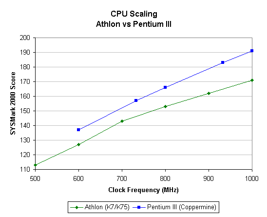
The above graph says it all: after the Athlon 700, there was a noticeable drop in the scaling of the processor's performance with clock speed. After the Athlon 700, the speed of the processor's L2 cache never dropped below 300MHz, but then again it never reached the 350MHz point it attained with the 700MHz part, which explains the clear difference in slope before and after the 700MHz point.
If that graph were to continue on, and AMD continued to release Athlon parts with higher L2 cache dividers, we would eventually see the performance leveling off while the Pentium III Coppermine would continue to scale linearly.
Luckily for AMD, the graph isn't going to continue on like that, since AMD is finally ready to introduce the long awaited successor to the Athlon, what we've known to be the Thunderbird, along with its full speed on-die L2 cache.
The History
The Athlon was the first non-Intel x86 processor to move from the conventional socketed design of the time (Pentium MMX, K6, K6-2, K6-III) to a slot-based interface connector, commonly known as Slot-A. The reason behind the move to a slot-based design was to enable the Athlon to feature a fast L2 cache that would remain on the processor card itself, thus removing the bottlenecks that having the L2 cache on the motherboard caused in the earlier days of Socket-7 motherboards.
The 0.25-micron Athlon die already took up a whopping 184 mm^2 of surface area and there was definitely no room for an on-die L2 cache, so the L2 cache remained on the processor card. With the release of the Athlon 750, AMD presented the first modification to the Athlon core, which was the move to a 0.18-micron die fabrication process, which reduced the surface area of the newly codenamed K75 core from 184 mm^2 to 102 mm^2, or 55% of the original die size.
The 0.18-micron manufacturing process allowed AMD to scale up to higher clock speeds, since the processor's heat and power consumption statistics were noticeably reduced; unfortunately, the fact that AMD had to rely on third party manufacturers to produce the Athlon's high speed L2 cache limited the growth potential of the Athlon.
The next step in the Athlon's progression was to take advantage of the smaller die size of the K75 core and integrate the L2 cache onto the die itself. By placing the L2 cache on the die of the Athlon, the latency of the L2 cache can be improved since it is much easier for the CPU to access the L2 cache if its physically located on the die of the CPU rather than if its located off of the CPU on the processor card itself.
Having the L2 cache on the die also allows it to operate at the same frequency as the rest of the die, meaning that it runs at the core clock speed of the CPU. The main benefit of this is that it allows the CPU's performance to scale properly with clock speed since, for every increase in clock frequency, you get a similar increase in L2 cache frequency as well.
The Basics
The Thunderbird will still use the name Athlon, but in order to distinguish it from the older Athlons (based on the K7 and K75 core), we'll refer to it as the Thunderbird. Keep in mind that when you go out to buy one, it should be listed as an Athlon. We'll get into the ways to differentiate the part numbers between the older Athlons and the new Thunderbird-based Athlons later in this article, but first, the basics.
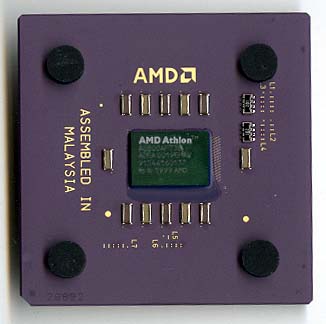
Currently, the Thunderbird itself is being released at 750MHz, 800MHz, 850MHz, 900MHz, 950MHz and 1GHz. This doesn't mean that there won't be slower OEM parts floating around; for the most part you can expect to see 750MHz – 1GHz Thunderbird parts available almost immediately. At 850MHz and slower clock speeds the Thunderbird runs at a core voltage setting of 1.70v, but at 900MHz and greater the voltage is set to 1.75v.
The Thunderbird features a full 256KB of on-die L2 cache that operates at clock speed, meaning that, on a Thunderbird 750, the core and the L2 cache both operate at 750MHz. This is in contrast to the original Athlons that operate their L2 cache at a certain fraction of the core clock speed; in the case of the Athlon 750, its external 512KB of L2 cache runs at 300MHz.
Integrating the 256KB of L2 cache on-die increases the die size of the 0.18-micron Athlon core by about 20%, which still makes the Thunderbird with 256KB of integrated L2 cache a smaller die than the original 0.25-micron Athlon. More specifically, the Thunderbird features a 120 mm^2 die size, compared to the 184 mm^2 die of the original Athlon (0.25-micron) and the102 mm^2 of the K75 Athlon (0.18-micron). In comparison, Intel's upcoming Willamette is rumored to have a die size of around 170 mm^2.
Adding the 256KB of L2 cache to the die of the Athlon also dramatically increases the transistor count of the CPU. As you remember from the original Athlon's release, the core weighed in at a hefty 22 million transistors. The new Thunderbird features a 37 million transistor core, meaning that the additional 15 million transistors on the Thunderbird are for the integrated L2 cache. This is compared to the 9.5 million (106 mm^2) Pentium III (Katmai) core and the 28 million (128 mm^2) Pentium III (Coppermine) core.
All those transistors switching rapidly translates into quite a bit of heat output. While AMD didn't have an exact value for us by press time, they did let us know that the Thunderbird should dissipate in the vicinity of 50W for the higher speed grades. In contrast, the original 0.25 micron Athlon 700 dissipated 50W as does an 0.18 micron Athlon 850. The Pentium III 1 GHz, on the other hand, dissipates just 33W.
|
CPU
Specification Comparison
|
|||||||
|
AMD
Athlon
|
Intel
Pentium III
|
Intel
Celeron
|
|||||
| Core |
K7
|
K75
|
Thunderbird
|
Katmai
|
Coppermine
|
Mendocino
|
Coppermine128
|
|
Clock Speed |
500
- 700 MHz
|
750
- 1000 MHz
|
450
- 600 MHz
|
500
- 1000 MHz
|
300
- 533 MHz
|
533
- 600 MHz
|
|
| L1 Cache |
128KB
|
32KB
|
|||||
| L2 Cache |
512KB
|
256KB
|
512KB
|
256KB
|
128KB
|
||
| L2 Cache speed |
1/2
core
|
2/5
or 1/3 core
|
core
clock
|
1/2
core
|
core
clock
|
||
| L2 Cache bus |
64-bit
|
256-bit
|
64-bit
|
256-bit
|
|||
| System Bus |
100 MHz DDR (200 MHz effective) EV6
|
100
- 133 MHz GTL+
|
66
MHz GTL+
|
||||
| Interface |
Slot-A
|
Socket-A
Slot-A (OEM only) |
Slot-1
|
Slot-1
Socket-370 |
Socket-370
|
||
| Manufacturing Process |
0.25
micron
|
0.18
micron
|
0.25
micron
|
0.18
micron
|
0.25
micron
|
0.18
micron
|
|
| Die Size |
184
mm^2
|
102mm^2
|
120mm^2
|
128mm^2
|
106mm^2
|
153mm^2
|
106mm^2
|
| Transistor Count |
22
million
|
37
million
|
9.5
million
|
28
million
|
19
million
|
28
million
|
|
The performance benefits of simply adding an on-die L2 cache are application specific, but it mainly allows the Athlon to reach much higher clock speeds and gain much more from those clock speeds than it otherwise would if it had a slower L2 cache running at 1/3 of the processor's frequency.
According to AMD, the on-die L2 cache of the Thunderbird core features a 45% lower latency than the older Athlons with their external L2 cache. The actual drop in latency was from 21 clock cycles on the older Athlons to 11 clock cycles on the Thunderbird.
In spite of the fact that the older K7 and K75 Athlon cores featured a larger 512KB external L2 cache, the integrated 256KB of L2 cache on the Thunderbird is actually faster than its predecessor because the L2 cache is running at such a higher frequency. While there will be some situations in which the larger L2 cache of the K7/K75 may come in handy, such as with database servers, for the most part the Thunderbird will prove to be faster than the regular Athlon because of its faster low latency L2 cache.
The final benefit of having an on-die L2 cache offers is that it removes the need for the processor card that the Athlon was otherwise required to have because of its external L2 cache chips. This helps to decrease the overall cost of the Athlon since you no longer have to pay for the processor card as well as the manufacturing costs associated with mounting a processor on the card itself.
It also paves the way for the Athlon to make the move to a socketed CPU interface, which would make the new Thunderbird the first socketed AMD CPU since the K6-X line of processors.
Thunderbird's L2 vs. Coppermine's L2
You'll notice that in AMD's press releases, they refer to the Thunderbird as having a total of 384KB of cache. This figure is derived by simply adding the 128KB of L1 cache that the Thunderbird still has from the original Athlon to the 256KB of L2 cache that is now on-die with the Thunderbird.
So what's different about the caching system of the Thunderbird versus that of the Coppermine? AMD is employing an exclusive cache architecture on the Thunderbird instead of the more conventionally used inclusive cache architecture, which is what Intel uses on the Coppermine.
Basically with an inclusive cache, all of the data that is stored in the L1 cache is duplicated in the L2 cache. While the Pentium III (Coppermine) features a 256KB on-die L2 cache, the data contained within its 32KB L1 cache is duplicated in the 256KB L2 cache.
An exclusive cache, which, as you can tell by the name, is the opposite of an inclusive cache, doesn't duplicate L1 data in the L2 cache area. The L2 cache only contains the copy-back cache blocks that are to be written back to the memory sub system (basically everything that doesn't fit in L1 and would normally go to the system memory if there was no L2 cache). Therefore, when AMD claims that the new Thunderbird core has a total of 384KB of on-die cache, they aren't lying; any data in the Athlon's (Thunderbird) 128KB L1 is not duplicated in its 256KB L2.
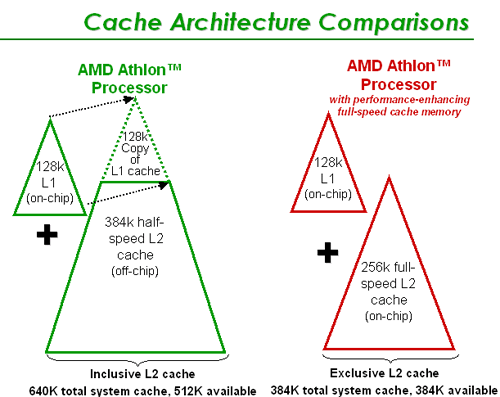
The Thunderbird still features a 64-bit data path to and from its L2 cache, which is unchanged from the original Athlon. This is a narrower data path than the Pentium III Coppermine's L2 cache has (256-bit vs. 64-bit), which could influence the performance increase the Thunderbird achieves over the original Athlon versus the improvement that we noticed with the Coppermine over the original Pentium III. This offers approximately 1/4 the L2 cache bandwidth of the Pentium III Coppermine which could definitely hinder performance.
Another difference between the Thunderbird's L2 cache and the Coppermine's L2 cache is that the Thunderbird features a 16-way set associative L2 cache whereas the Coppermine features an 8-way set associative L2 cache. What exactly does that mean? In order to explain that we need to take a look at what L2 cache actually does.
L2 Cache: What it does
We often take for granted that having an L2 cache means that your system runs faster than it would if it wasn’t there, but what does that L2 cache actually do?
L2 cache, just like any other cache, acts as sort of a middle man between two mediums, in this case, your CPU’s L1 cache and your system memory (as well as other storage mediums). When the CPU wants to request a bit of data, it first searches in its L1 cache to see if it can find it there; if it does, then this results in what is known as a cache hit and the CPU retrieves it from the extremely fast, low latency L1 cache.
If it can’t retrieve it from L1 cache, it then goes to the L2 cache where it attempts to do the same – obtain a cache “hit.” In the event of a miss, the CPU must then go all the way to system memory in order to retrieve the data it needs. With the L2 cache of today’s CPUs operating at a much higher frequency and at much lower latency than system memory, if the L2 cache weren’t there or the cache mapping technique wasn’t as effective, we would see considerably lower performance figures from our systems.
Cache Mapping Techniques
We just established that the function of the L2 cache is to provide access to commonly used data in system RAM. It does so by essentially mapping the cache lines of the L2 cache to multiple addresses in the system memory (the number of which is defined by the cacheable memory area of the L2 cache).
There are a number of methods that can be used to dictate how this mapping should occur. On one end of the spectrum, we have a direct mapped cache, which divides the system memory into a number of equal sections, each one being mapped to a single cache line in the L2 cache.
The beauty of a direct mapped cache allows it to be searched relatively quickly and effectively since everything is organized into sections of equal size, but with this comes the sacrifice of hit rate because the technique does not allow for any bias toward more frequently used sections of data.
On the other end of the spectrum, we have a fully associative cache, which is the exact opposite of a direct mapped cache. Instead of equally dividing up the memory into sections mapped to individual address lines, a fully associative cache acts as more of a dynamic entity that allows for a cache line to be mapped to any section of system memory.
This flexibility allows for a much greater hit rate since allowances can be made for the most frequently used data. However, since there is no organized structure to the mapping technique, searching through a fully associative cache is much slower than through a direct mapped cache.
Establishing a mid-point between these two cache mapping techniques, we have a set associative cache, which is what the current crop of processors uses.
A set associative cache divides the cache into various sections, referred to as sets, with each set containing a number of cache lines. With an 8-way set associative L2 cache, each set contains 8 cache lines, and in a 16-way set associative L2 cache, each set contains 16 cache lines.
The beauty of this is that the cache acts as if it were a direct mapped cache except that, instead of the 1 cache line per memory section requirement, we get x number of cache lines per section of memory addresses.
This helps to sustain a balance between the pros and the cons of a direct mapped and a fully associative cache.
In the case of the Thunderbird and the Pentium III Coppermine, the 16-way set associative L2 cache of the Thunderbird allows for a higher hit rate for the L2 cache than the 8-way set associative L2 cache of the Pentium III Coppermine. In comparison, the older Athlons featured a 2-way set associative L2 cache.
Aluminum vs. Copper
One of the biggest revelations that was made about the Thunderbird before its official launch was that it would employ the use of Copper interconnects rather than the more conventional Aluminum. It later became evident that only some of the products carrying the Athlon name would feature Copper interconnects while others would continue to use Aluminum.
The reason for the move to Copper is because it conducts electricity better than Aluminum. Unfortunately, you cannot manufacture both Aluminum and Copper-based processors in a single plant, so AMD's Fab25 plant in Austin, TX, which has been manufacturing Aluminum based processors, cannot produce Copper Thunderbirds. Luckily, AMD's Fab30 plant in Dresden, Germany is capable of producing Copper-based processors. Since the Thunderbird does not require that it be produced on a Copper process, both Austin and Dresden will be producing Thunderbird CPUs.
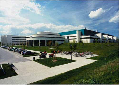
There shouldn't be any performance differences between Copper and Aluminum-based Thunderbirds, so there's no reason to worry about getting a part from Dresden versus getting one from Austin. Since both the Copper and Aluminum parts will operate at the same core voltage, their thermal characteristics should be similar as well. So what then is the point for moving to Copper interconnects?
As AMD moves to finer manufacturing processes, in the future, the Copper interconnects will definitely play an important role as AMD approaches higher clock speeds.
Whether you get a Dresden made copper-Thunderbird or an Austin-made aluminum part is pretty much up to the luck of the draw. For example, our 1GHz Thunderbird part came from Dresden (Copper) while our 800MHz part came from Austin (Aluminum).
AMD did mention to us that only the high performance parts would be manufactured out of Dresden for now, meaning that the upcoming Duron will be manufactured entirely out of Austin. The reasoning behind this is that AMD's goal with the Duron is to crank out as many as possible and the easiest way to do that is to produce them on a process that is tried and true. In addition, there's no reason to use copper interconnects on a processor that isn't scheduled to really hit high clock speeds anytime soon.
Socket-462 vs. Slot-A
As we mentioned earlier, by placing the L2 cache on the die of the Athlon itself, there was no longer a need for the Athlon's processor card, which paves the way for the introduction of the socketed Athlon, more specifically the Socket-462 interface.
The Socket-462 interface has the same physical dimensions as a Socket-7 or a Socket-370 socket, which allows it to use the same cooling fans and clips that are used on Socket-7 and Socket-370 coolers.
One thing you'll notice about the Socket-462 interface is that there are some missing pins in the otherwise full layout. The reason for this is to prevent the accidental insertion of a Socket-370 processor into the socket since the missing pin holes line up with physical pins on all Socket-370 CPU.
The Thunderbird will be available primarily in a Socket-462 package since AMD is very intent on making the move to the cheaper socketed packaging on all of their processors. However, in order to support the OEMs that already have Slot-A system designs, AMD will be shipping limited quantities of the Thunderbird in a Slot-A package, which is basically identical to the older Athlons with the exception that it has no L2 cache chips on the processor card itself.
We pointed out not too long ago that, although the Thunderbird will be available in a Slot-A package, for most end users it will be much easier finding a Socket-462 Thunderbird than it will be finding a Slot-A part. The Slot-A parts are supposed to be allocated to OEMs alone and only in limited quantities, so while you may see them pop up on various vendors' sites online, don't expect to see them as readily available as the Socket-462 parts.
The situation gets even more complex when you take into account that the only Slot-A chipset that officially supports the Thunderbird is the AMD 750. It was discovered early on that there was the potential for motherboards based on the VIA KX133 chipset to have compatibility problems with the limited number of Slot-A Thunderbirds in production.
The only possible explanation for the ability of the Thunderbird to be guaranteed to work with the AMD 750 chipset but not with the KX133 is because the KX133 reference design features timing specs that are out of the Thunderbird's range. This could also explain why certain motherboard manufacturers are claiming that their KX133 settings work fine with the Slot-A Thunderbirds; basically, if a KX133 motherboard manufacturer is claiming their board will work fine with a Slot-A Thunderbird, they're probably just increasing the tolerance the board has for out of spec signals or boosting the signal strength going to the processor itself.
Chipset Support
So if the VIA KX133 doesn't officially support the Thunderbird, then what chipsets do? Aside from the original AMD 750 chipset, VIA does have a Socket-462 version of their KX133 chipset, the KT133.
The KT133 is exactly the same as the KX133 chipset in that it uses the same memory controller, the same AGP controller, and basically is the same North Bridge with slight timing modifications to support the Socket-462 Thunderbird processor.
VIA will be releasing a version of the KT133 chipset with a Savage4 AGP device integrated into the North Bridge of the chipset. As far as we know, this will be called the KM133 chipset and it's pin compatible with the KT133's North Bridge. The KM133 also features an on-board AGP 4X slot, so that, if you're not going to use the integrated Savage4 graphics, you can simply stick in a regular AGP (or PCI for that matter) video card and it will disable the integrated device.
For those of you that need a refresher on what features the KX133 and thus KT133 chipsets support, let's take a look at the explanation behind the specs of the North and South Bridges that the chipset uses:
VT8363 North BridgeThe KT133 uses a slightly different North Bridge than the KX133, the 8363 instead of the 8371 that's a part of the KX133 chipset.
· High Performance Athlon CPU Interface – All that this fancy statement means is that the 8363 interfaces with the Socket-A connector on the motherboard using the Athlon’s EV6 bus. This interface is the "200MHz FSB" that most Athlon motherboard manufacturers throw around when it’s actually a 100MHz Double Data Rate FSB. This implementation remains relatively unchanged from the original AMD 751 North Bridge, meaning that the amount of available bandwidth has not changed (1.6GB/s).
· Fully Featured Accelerated Graphics Port (AGP) Controller – The 8363’s integrated AGP controller is actually borrowed from VIA’s 694X AGP controller in that they both feature the same core. The controller features support for AGP 1X, 2X and 4X transfer rates, and because of its AGP 4X support, motherboard manufacturers can choose to implement an AGP Pro connector on motherboards based on the KT133 chipset. This is an improvement over the AGP 2X limitation of the AMD 751 North Bridge.
· Concurrent PCI Bus Controller – The integrated PCI controller is the same as the 694X’s (Apollo Pro 133A) PCI bus controller. It supports 5 PCI master devices, but motherboard manufacturers can implement more than 5 PCI slots, the added slots will simply be slave devices. Nothing special here.
·
Advanced High-Performance DRAM Controller – The Memory subsystem of the
KT133 is the biggest difference between the 8363
North Bridge and the AMD 751 North Bridge. The 8363 can address up to 8 RAS lines, meaning
motherboard manufacturers can outfit their boards with up to 4 DIMM slots with
support for double sided DIMMs in all of the slots.
The memory controller, once again, very closely resembles that on the 694X (Apollo
Pro 133A), especially in the supported memory types. The 8363
currently only supports PC133 and PC100 SDRAM (no
DDR SDRAM
support) as well as VC133 and VC100 Virtual Channel SDRAM support.
The memory bus can operate (officially) at either 100MHz or 133MHz, which is
an improvement over the sole 100MHz setting present on motherboards based on
the AMD 750 chipset. Keep in mind that we’re talking about the memory
bus frequency, not the front side bus frequency, the latter which
operates at 100MHz DDR regardless of the frequency of the memory bus.
The 133MHz memory bus frequency allows the KT133 to attain an available 1.06GB/s
of peak memory bandwidth, up from the 800MB/s on the AMD 750.
The chipset itself supports up to 2GB of memory, but it’s up to the motherboard
manufacturers to make sure that their boards can reach this capacity properly
without sacrificing stability.
The 686A was first introduced on the Apollo Pro 133 chipset but is referred to as an option on the old Apollo Pro, a P6 chipset, as VIA’s Super South Bridge, this of course being an improvement over the 596B regular South Bridge. The 686A has been paired up with the 693 North Bridge for use with the Apollo Pro+, again with the 693A North Bridge for the Apollo Pro 133, and once again with the 694X North Bridge of the Apollo Pro 133A.
The flexibility of VIA’s North/South Bridge setup is one reason they have kept it around for so long, and it has allowed them to use the 686A on their two Super7 chipsets, the MVP3 and the MVP4.
On the Athlon side of things, the 686A was the replacement South Bridge for the AMD 756 in some designs that implemented the AMD 750 chipset. The 686A was then featured on the KX133 chipset and now on the KT133 as well.
The 0.35-micron, 352-pin 686A remains unmodified from its original introduction and use on the P6 chipsets, and thus the specs remain the same. Let’s discuss the benefits of each one of these features to see what they actually accomplish:
· Inter-operable with VIA and other Host-to-PCI Bridges – As we just finished discussing, the fact of the matter is that the 686A can be used on a number of VIA chipset implementations, thus helping to keep costs down since VIA only has to manufacture one chip that can be implemented on a number of motherboard designs.
· Integrated PCI-to-ISA Bridge – This feature, present on the now old Intel piix4 and piix4e South Bridges but absent on the i820 and i810(E) chipsets, allows for the implementation of ISA slots on a motherboard that uses the 686A without having to use an external PCI-to-ISA Bridge. This helps save PCB space and cut costs. On the reverse side of things, ISA slots are quickly dying, so this feature is becoming less of a necessity.
· Ultra ATA 33/66 PCI EIDE Controller – Just recently, Ultra ATA 33 has began to be saturated by the latest 7200 RPM IDE hard drives, so Ultra ATA 66 support is definitely a desired feature. While Intel is supposed to announce ATA-100 support in the near future, it will be a while before hard drives saturate the 66MB/s peak transfer rates of the Ultra ATA 66 specification.
· Integrated Super I/O Controller – Unique to the 686A, the integrated Super I/O controller takes care of all of the basic I/O needs of a motherboard. It provides the serial, IR, and parallel ports as well as the Floppy Disk Controller for the motherboard. Why is this so special? Well, currently no Intel chipset has these features integrated into any part of the chipset, meaning they have to resort to an external I/O controller to provide these functions. This external controller not only occupies PCB area on the motherboard, but it also adds the cost of another chip to the price of the motherboard. This is a feature the AMD 756 South Bridge does not support, one reason why many motherboard manufacturers chose to go with the 686A over the AMD 756 in their Athlon motherboard implementations.
· AC’97 & MC’97 Support – KT133 motherboards that take advantage of the Audio Codec ’97 support of the 686A South Bridge will feature an AC’97 controller placed on the motherboard that drives an integrated audio output while supporting the use of the AMR (Audio Modem Riser) slot for higher quality audio or modem support. The reason for the use of the AMR slot is to place the more sensitive components on an AMR slot so that motherboard manufacturers don’t have to increase the production time of their products because of the certification required for sensitive analog components such as those on modems or higher quality audio devices. This is also why, in spite of the presence of the AMR slot, the motherboard manufacturers will go ahead and include audio inputs/outputs on the motherboard itself, so they don’t have to worry about the certification time required by an AMR card in order to ship their boards to OEMs with integrated sound.
Remember that these AC’97 controllers depend on the host CPU to do most of the work associated with their particular tasks, but because of this they add a negligible amount to the final cost of the motherboard.
· Integrated Hardware Monitoring – Once again, by integrating hardware monitoring onto the 686A South Bridge, VIA helps to cut motherboard manufacturing costs by removing yet another chip from the PCB. Most motherboards use an external chip to provide hardware monitoring functionality, which takes up PCB space and adds the cost of the chip to the motherboard. The integrated hardware monitoring can monitor 5 voltages (including the voltage supplied to the 686A chip itself), three temperatures (including the temp of the 686A), and two fans.
· Universal Serial Bus Controller – The 686A’s USB controller goes one step above Intel’s current USB implementation by allowing support for up to 4 USB devices.
In the end, the 686A South Bridge helps to integrate three commonly external chips (I/O Controller, Hardware Monitoring Controller, and South Bridge) into one chip.
Part Numbers & Buying a Thunderbird
Earlier on in the review, we mentioned that the Thunderbird would still fall underneath the Athlon name, basically meaning that now there are two types of Athlons that carry the same name. The Athlon 750 – 1GHz parts will be available in both regular Athlon and Thunderbird versions, so how can you tell the two apart?
First of all, don't assume that the difference will be price. AMD is hoping to make the transition to Thunderbird as quickly as possible, and what they're doing to help ensure that is by selling Thunderbird parts to vendors at the exact same price as older Athlon parts. Meaning that it costs as much for a vendor to purchase an older Athlon 800 as it does for them to purchase a new Thunderbird-based Athlon 800. This should translate into Thunderbirds being the exact same price as the regular Athlons, although some vendors may discount the older Athlons by a bit in order to rid themselves of any excess stock they may have.
The easiest way to tell the two CPUs apart is that the Thunderbirds will be advertised as a Socket-A processor, whereas the regular Athlons will simply be Slot-A parts. If you ask for a Socket-A Athlon, you're definitely going to get a Thunderbird (unless your vendor sells you a Duron which is also Socket-A, but that's a sign of a bad vendor).
Another way to make certain that you'll be getting a Thunderbird is to make sure to select an Athlon with 256KB of on-die L2 cache, as the regular Athlon is only available with 512KB of L2 cache.
If all of that fails (which it shouldn't), you can always look at the part numbers on the chips themselves. Here is a quick tutorial on what the part numbers mean.
The part number for the older Athlons followed this type of a scheme: AMD-K7XXX where XXX is the clock frequency. In the case of an Athlon 900, the part number would be AMD-K7900.
The part numbers for the newer Thunderbirds follow this type of a scheme: AMD-AXXXX where XXX is the clock frequency. In the case of a 900MHz Thunderbird, the part number would be AMD-A0900.
Overclocking
The Athlon, as well as all Pentium II and early Pentium III CPU's, have been limited in overclocking potential in part by the external L2 Cache chips. When Intel released its first CPU with on-die cache, the Celeron 300A, a new era in overclocking was upon us. No longer was it necessary to worry about cache speeds as that on-die cache scaled with the core clock thanks to it being built using the same process technology as the rest of the core.
Intel did the same for the Coppermine core used on the latest Pentium III's and, as stated earlier, AMD has done the same for the Thunderbird. Does that mean the Thunderbird is an overclocking monster like some of the Celeron and Pentium III models with on-die cache? Well there's a lot more to overclocking than just on-die cache, although the limits of external cache speed has prevented overclockers from pushing their Athlon's to the max.
Overclocking the Athlon in the past was accomplished most easily with a "Gold Finger Device" that allowed you to adjust the multiplier of any Slot-A Athlon. If you haven't heard the rumors by now, the Thunderbird, as well as all future Socket-A CPUs including the Duron, is multiplier locked, meaning that you cannot adjust the multiplier of the CPU.
Currently, it seems as if AMD is using a technique similar to what Intel has been doing with their processors ever since the release of the Celeron, thus completely locking them. It is highly unlikely that there will be any way around this, thus limiting the overclocking potential of the new Thunderbirds to what you can do with simply increasing the FSB.
Traditionally, we've only been able to push the EV6 bus to about 110MHz, whether it be on a KX133 or an AMD 750 based motherboard. Before we even had our CPU's in hand, we know that this was likely to limit the overclocking potential of the Thunderbird. The 8363 North Bridge of the KT133 is very similar to the 8371 used on the KX133 so the maximum attainable FSB speed probably won't change much. The AMD 760, expected later this year, is expected to introduce a 133 MHz DDR (266 MHz effective) version of the EV6 bus and should enable a number of overclocking options for the Thunderbird.
At the time of publiciation, we had two Thunderbird samples to play around with. Running at 1 GHz and 800 MHz meant that we had CPU's with a multiplier of 10X and another with a multiplier of 8X. Motherboard selection was also limited, with about 5 pre-production models available to us. These factors conspired to prevent us from overclocking our Thunderbirds beyond 1.05 GHz and 840 MHz using a 105 MHz FSB speed. Even with such a mild overclock, the systems were not 100% stable under these conditions. The fact that both CPU's topped out at an FSB speed of 105 MHz seems to indicate that there may be hope for the Thunderbird to overclock more than 5% once final boards are available, but only time will tell.
The Test
|
Windows 98SE / 2000 Test System |
|||||
|
Hardware |
|||||
|
CPU(s) |
Intel
Pentium III 800E |
Intel
Pentium III 800
Intel Pentium III 733 Intel Pentium III 667 Intel Pentium III 600EB |
AMD
Athlon (Thunderbird) 1000
AMD Athlon (Thunderbird) 800 AMD Athlon 1000 AMD Athlon 900 AMD Athlon 800 AMD Athlon 700 AMD Athlon 600 AMD Athlon 500 |
||
| Motherboard(s) | AOpen AX6BC Pro Gold | AOpen AX6C | ASUS P3V4X | VIA
KT133 Reference |
ASUS K7V |
| Memory |
128MB PC133 Corsair SDRAM |
128MB
PC800 Samsung RDRAM
|
128MB
PC133 Corsair SDRAM
|
128MB
PC133 Corsair SDRAM
|
|
| Hard Drive |
IBM Deskstar DPTA-372050 20.5GB 7200 RPM Ultra ATA 66 |
||||
| CDROM |
Phillips 48X |
||||
| Video Card(s) |
NVIDIA GeForce 2 GTS 32MB DDR (default clock - 200/166 DDR) |
||||
| Ethernet |
Linksys LNE100TX 100Mbit PCI Ethernet Adapter |
||||
|
Software |
|||||
|
Operating System |
Windows
98 SE |
||||
| Video Drivers |
|
||||
|
Benchmarking Applications |
|||||
| Gaming |
GT
Interactive Unreal Tournament 4.20 AnandTechCPU.dem |
||||
| Productivity |
BAPCo SYSMark
2000 |
||||
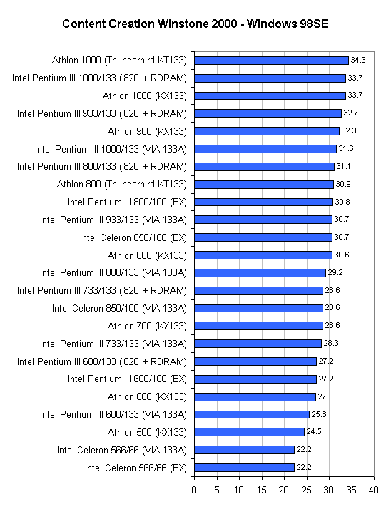
Before the introduction of the Thunderbird, the 1GHz Athlon was pretty much tied with the 1GHz Pentium III under Content Creation Winstone 2000. Now with the release of the Thunderbird we see a slight advantage tossed to AMD although the performance improvement we're measuring here isn't all that great at all.
We have a number of different platforms present in the above graph, but if you're truly interested in a CPU to CPU comparison the best way to do that would be to look at the Athlon on a KX133/KT133 and compare it to the Pentium III on a VIA 133A since the two chipsets share the same AGP and memory controllers. If you look at it like that, then there is a clear performance advantage that the Athlon holds over the Pentium III.
The i820 + RDRAM platform does crowd things a bit while giving the Athlon more competition, but basically in this test you're coming away with a couple percent gain in performance simply by moving the L2 cache onto the die of the processor and increasing its clock speed.
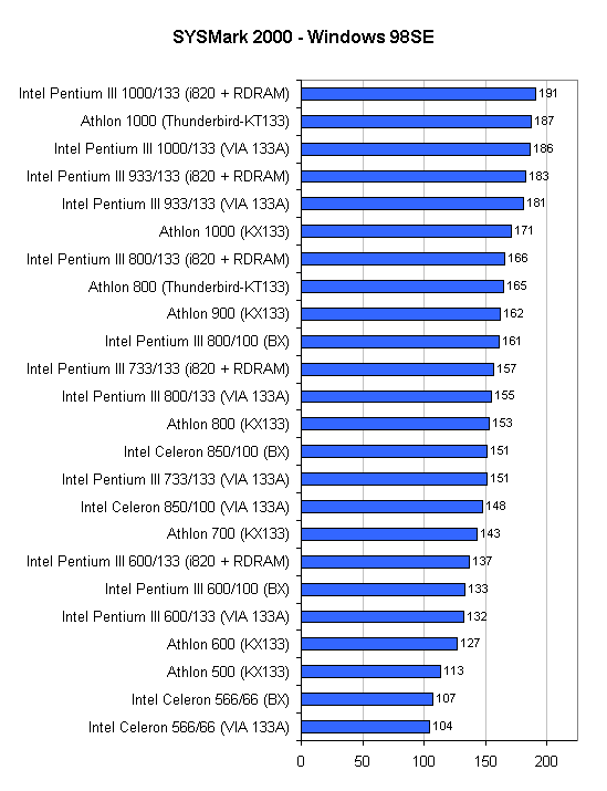
Under SYSMark 2000 we can finally start to see a decent increase in performance courtesy of the Thunderbird's full speed on-die L2 cache. One of the many factors that was penalizing the Thunderbird under SYSMark 2000 was the fact that its L2 cache was always running at or below 350MHz and one of the known traits of the benchmark is that it has a strong bias towards a fast memory subsystem and a fast L2 cache as well.
Simply by moving the L2 cache on-die and increasing its clock speed the Thunderbird manages to pull away with a 10% improvement in performance under SYSMark 2000. While this doesn't put the Thunderbird at the very top of the chart it places the CPU very close to the Pentium III 1GHz (820) forerunner which is considerably more expensive.
This 10% performance improvement is on the lower end of what we were told by AMD to expect from the Thunderbird seemingly ages ago, a 10 - 20% improvement in performance was what we could expect from the move to an on-die L2 cache running at clock speed.
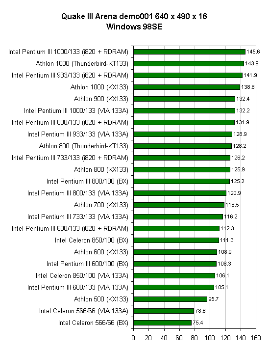
The Thunderbird manages to pull ahead of the regular Athlon by a little bit once again, under Quake III Arena the improvement is approximately 4%. While that is far from impressive, do keep in mind that the Athlon already has a fairly hefty L1 cache that has allowed it to perfom very well in spite of its prior lack of a high speed, low latency L2 cache.
Once again for a true clock for clock CPU comparison you'd have to compare the Athlon on the KX133/KT133 to the Pentium III on a VIA 133A since the two share the same memory/AGP controller in which case the benchmarks speak for themselves. But that comparison also illustrates exactly how limited the Athlon is by its platform, with a faster memory controller and a better overall designed chipset the Athlon would most definitely pull ahead even further. But because it's being held back by the KX133/KT133 the Pentium III on the 820 platform ends up on top.
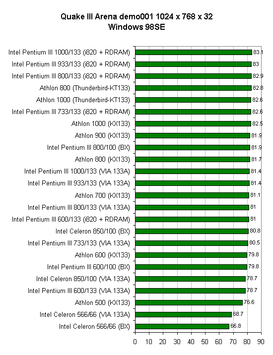
At this high of a resolution the GeForce 2 GTS we used in the tests became the limiting factor. This just goes to show you that if you're interested in playing a game at the point where the video subsystem becomes the limitation, it doesn't really matter what CPU you get as long as it is fast enough so that you aren't CPU limited before you are video card limited.
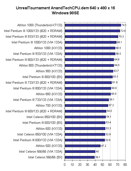
UnrealTournament definitely goes to the Thunderbird. Prior to the Thunderbird's release the Pentium III on the 820 platform easily dominated the UnrealTournament tests, as you can tell by the above graph even the Pentium III on the VIA Apollo Pro 133A chipset manages to beat out the original Athlon running at 1GHz on a KX133. Simply moving to the Thunderbird + KT133 platform results in an 11% improvement in performance which is definitely noticeable during normal gameplay.
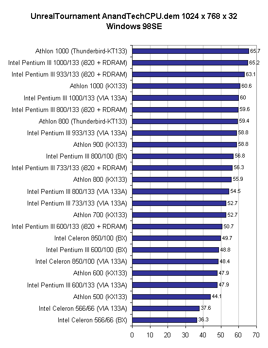
While the GeForce 2 GTS still fails to be a overly limiting factor even at 1024 x 768 x 32, the added memory bandwidth and fill rate required to drive frame rates above 60 fps in this test help to take down the Thunderbird's performance advantage over the original Athlon to around 8%.

Expendable is a situation where raw processing power matters more than having a fast L2 cache, which is the only real advantage the Thunderbird brings to the table in addition to what the Athlon can already boast. For this reason you don't notice a huge performance increase between the 1GHz Athlon and the new 1GHz Athlon running on the Thunderbird core.
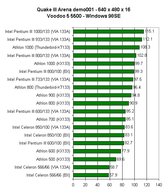
By benchmarking on a Voodoo5 we isolate the CPU a bit more by removing the T&L that the GeForce 2 GTS provides. The Pentium III clearly comes out ahead on a clock for clock basis, even "crippled" by the VIA 133A platform. Since this was not the case with the GeForce 2 GTS, there are a couple possible explanations. Either the Voodoo5 drivers SSE optimizations are better than their 3DNow! optimizations, the Pentium III SSE is actually faster than the Athlon 3DNow!, or the Pentium III is actually better at performing the T&L calculations that the GeForce 2 GTS was performing previously. While the drivers used here were final shipping versions, there is always room for improvement in the future.
The Thunderbird's low latency cache does give an 8% performance improvement compared to the original Athlon at similar clock speeds. This compares with the 4% improvement we saw with the GeForce 2 GTS.
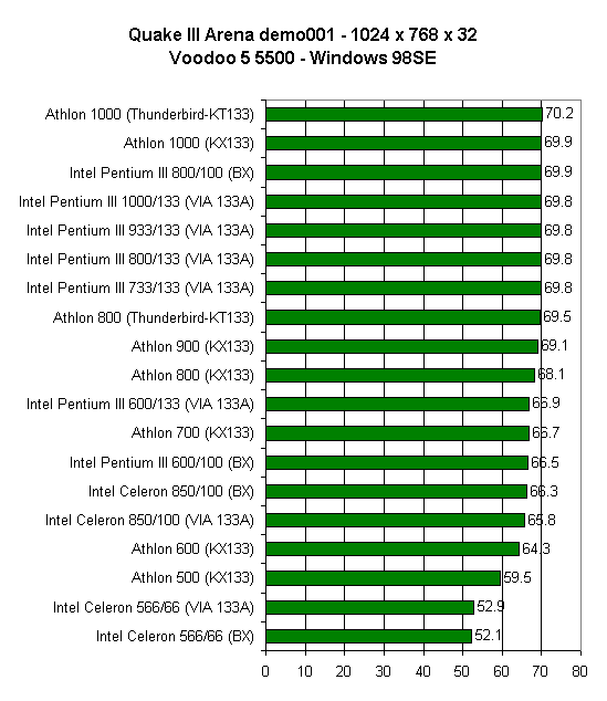
At 1024x768x32, we see the fillrate of the Voodoo5 5500 become the bottleneck, just as we did before. Basically, everything performs the same with the exception of the slowest CPU's.
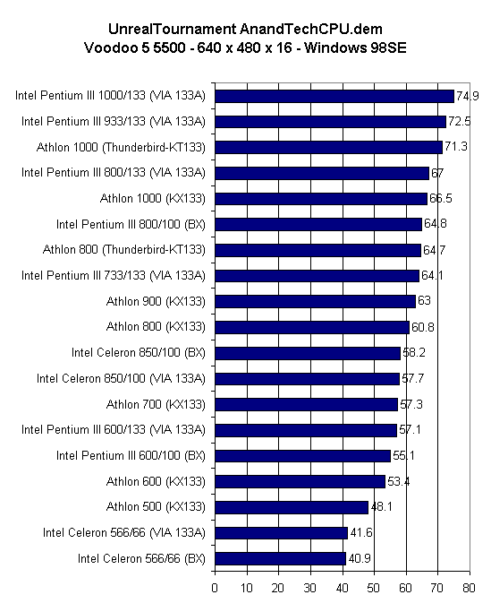
UnrealTournament shows basically the same result as Quake III at 640x480x16, but with less variation from top to bottom. This time, however, we can't blame the performance difference on anything related to T&L since UT does not take advantage of this feature.
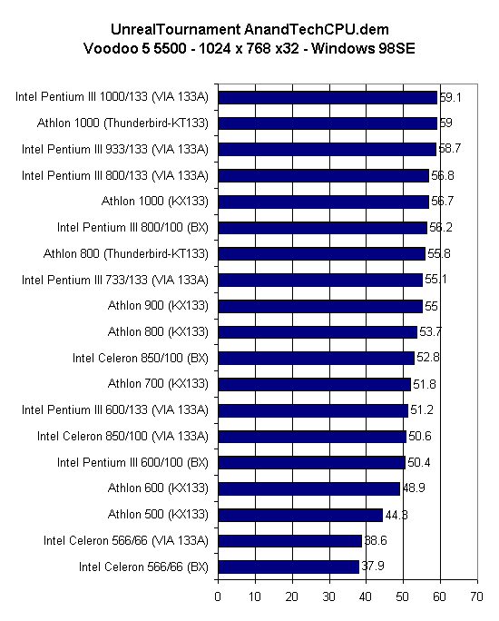
Fillrate limitations once again kick in at 1024x768x32, but UnrealTournament still scales somewhat with CPU speed at this resolution.
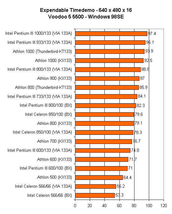
Expendable once again shows that the low latency L2 Cache of the Thunderbird makes very little difference compared to the original Athlon in certain situations.
Interestingly, the Pentium III and Athlon have again switched places, with the Pentium III taking the lead on a clock for clock basis. Apparently the Voodoo5 gets along better with Intel processors than AMD ones.
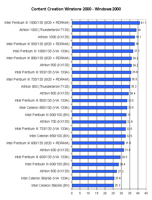
With this review, we've replaced Windows NT 4.0 with Windows 2000. With Content Creation Winstone 2000, we can see a performance boost across the board that Windows 2000 provides thanks to its NT roots.
The Pentium III teamed with 820 + RDRAM manages to steal the lead from the Thunderbird, while the VIA 133A moves up a bit in the rankings to overtake the non-overclocked BX. We still see both Athlon models well ahead of the Pentium III when compared on the VIA platforms, emphasizing that the Athlon is probably limited by its VIA chipset. The performance delta between Thunderbird and the original Athlon is larger than under Windows 98SE, but still relatively small.

Under High End Winstone 99, the low latency L2 of the Thunderbird allows the Athlon platform to leap frog the Pentium III, even with RDRAM, and take the top spot. Even the 800 MHz Thunderbird came out on top of the original Athlon 1 GHz. Once again, the performance improvement is in the vicinity of 8%.
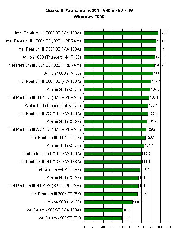
We've noted in the past that the AGP GART driver included with Windows 2000 has severely hindered performance of VIA-based platforms in gaming situations. In the past few days, VIA has finally released an updated AGP GART driver for Windows 2000 that helps performance considerably.
The Pentium III, regardless of platform manages to push out ahead of the Thunderbird. It's interesting to note that the VIA 133A actually overtakes the 820 + RDRAM and the non-overclocked i440BX thanks to that new AGP GART.
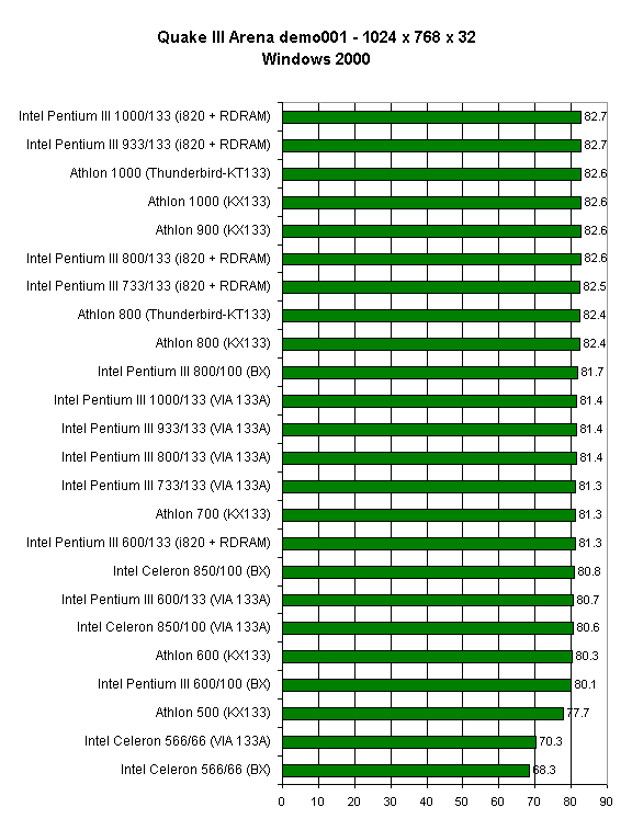
The fillrate limitations of the GeForce 2 GTS once again dominate the 1024x768x32 scores on all but the slowest CPU's.
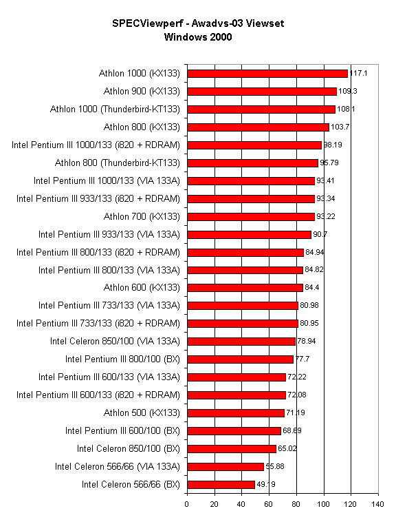
Ever since the Athlon has been teamed with the KX133 chipset, it has been able to completely dominate most of the SPECViewperf benchmark suite. While Thunderbird is no exception, it actually comes out a bit slower than the original Athlon. One possible explanation is the immature nature of the KT133 platform. This is somewhat surprising considering the similarity of the KT133 to the KX133. The other possibility is that a larger L2 cache is more important than a fast L2 cache under these circumstances.

The results are the same here, but the Pentium III with RDRAM is finally able to edge out the Athlon 900.
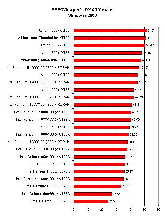
Under the Data Explorer test, the Pentium III needs RDRAM to edge out even an Athlon 600.
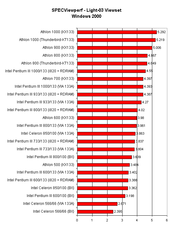
The same goes for the Lightscape test, but this time the Pentium III GHz with RDRAM is barely able to beat out the Athlon 700.
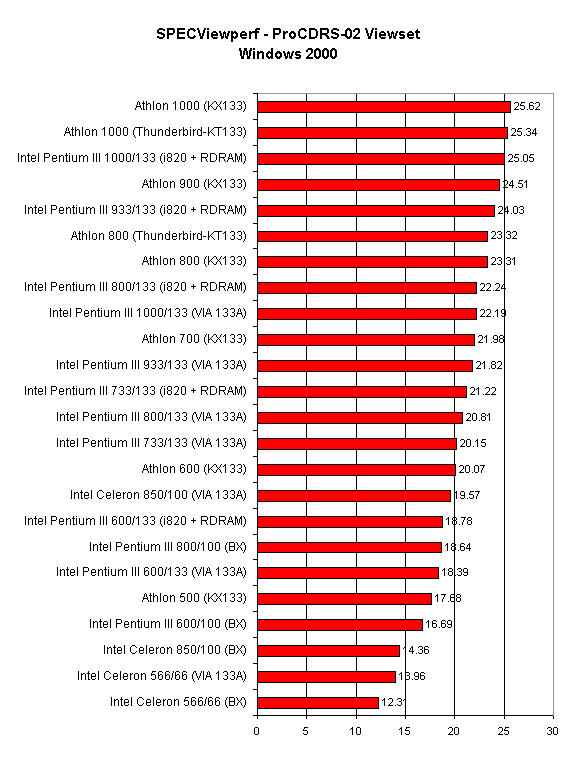
The results are the same under the ProCDRS test as well. Clearly AMD is doing something right in order to dominate these professional benchmarks as much as they are. It is nevertheless somewhat surprising that the Thunderbird falls behind the original Athlon. As noted previously, it maybe the immaturity of the KT133 boards used for testing or it may just be the larger cache of the original Athlon.
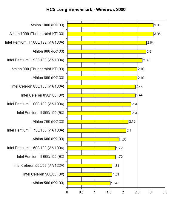
By popular request, we'll be including RC5 benchmarks in CPU reviews starting today. For those that don't know, the RC5 is a form of encryption. Distributed.net is holding a challenge to crack the RC5 encryption to show that it is weak and encourage the implementation of stronger security. Click here to learn more about the Distributed.net challenge and join Team AnandTech for the opportunity to win $1000.
L2 cache speed clearly does not matter in this purely CPU intensive benchmark as can be seen by the identical scores of the Thunderbird and original Athlon at the same clock speed. It's also interesting to note that the platform used here makes absolutely no difference with regards to performance - raw CPU power is the key here as evidenced by the exact double performance of the 1 GHz Athlon/Thunderbird compared to the Athlon 500. Once the Duron is available, it will be the ideal CPU for cracking RC5.
Conclusion
If you were expecting the Thunderbird to completely wipe away the competition then you're most likely going to be dissappointed by its performance. However if you understand that the whole point for moving the Athlon's L2 cache on-die was to make way for higher clock speeds without diminishing performance returns, then the Thunderbird makes a much more lasting impression.
Considering that the Thunderbird is going to be priced the same (from AMD at least) as the older Athlons there is no reason for you to want to purchase an older Athlon unless vendors begin discounting them heavily. However if you're currently an Athlon owner, the investment you made in your processor is probably too great to just throw away so you can get a Thunderbird. The performance improvement over the Athlon is not great enough to make you want to upgrade if you already have an Athlon running (either regularly clocked or overclocked) at 700MHz or above.
The fastest official platform for the Pentium III is still the i820 + RDRAM setup which is still entirely too expensive to justify the relative lack of a performance increase over competing platforms. Clock for clock the Thunderbird is generally faster than the Pentium III on all of its official platforms (BX, 820, 133A) although in some cases the Thunderbird is edged out by the Pentium III on an 820 + RDRAM setup.
If you compare the Thunderbird on a KT133 motherboard to a Pentium III on a VIA 133A motherboard you can see that the Athlon holds a large advantage over the Pentium III, but you can also see that the Athlon is being severely limited by the performance of the KT133 chipset. Compared to the BX and 820 chipsets the VIA 133A definitely lags behind, and since the KT133 is based on the same AGP core and features the same memory controller as the VIA 133A you can expect to see the same subpar performance with that part as well. If you compare the Athlon on a KT133 platform to an overclocked BX133 setup you will truly be able to see how much of a limitation the KT133 chipset is for the Thunderbird.
Unfortunately there is not much hope in the near future for the Thunderbird chipset situation. The next big chipset release that you'll want to watch out for will most likely be AMD's 760 chipset which will be released around the time of the Mustang core. The chipset itself, will support DDR SDRAM and the 133MHz DDR FSB (effectively 266MHz) and should provide everyone with the performance improvement we've been hoping for. If you currently have an Athlon, the release of the AMD 760 chipset is probably when you'll want to upgrade your setup if you were thinking about doing so.
In a couple of weeks we will be releasing performance figures on AMD's Duron, their low-cost version of the Athlon. For those of you that are about to dive into the Athlon platform you may want to wait until Duron is released before making your final decision. If you're already content with the benchmarks you see for the older Athlons (512KB L2) then the Duron may be all that you need since it will generally perform between 90 - 100% of the speed of an equivalently clocked Athlon (not Thunderbird). The major benefit the Duron has going for it is its extremely low cost, there is no question that the Duron will end up dominating the low end market where Intel's Celeron has failed to perform as well as we expected.
To summarize this all, if you want the fastest Athlon then go for the Thunderbird, if you were about to purchase an Athlon wait for the Duron, it's just about as fast, and if you're currently an Athlon owner wait for the AMD 760 chipset before upgrading, it's not worth it right now. If you're borderline between purchasing an Athlon or a Pentium III, the latter will only hold a major performance advantage if you're going to be running on an overclocked BX platform. Otherwise the decision is pretty much a toss up and one that only you can make for yourself. The only suggestion we can make is to stay away from the 820 + RDRAM platform for now, it is entirely too expensive for an end user; unless the price of RDRAM comes down there is no reason to pursue the platform. The best chipset for the Pentium III still seems to be the BX, albeit in overclocked form, so if you're going to be going down the Pentium III route you're probably better off using a BX based board.


