Original Link: https://www.anandtech.com/show/5193/intel-and-micron-imft-announce-worlds-first-128gb-20nm-mlc-nand
Intel and Micron (IMFT) Announce World's First 128Gb 20nm MLC NAND
by Anand Lal Shimpi on December 6, 2011 12:17 PM EST

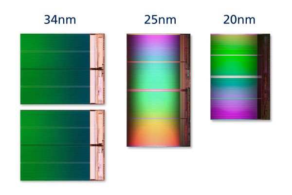
Earlier this year, Intel and Micron's joint NAND manufacturing venture (IMFT) announced it had produced 64Gb (8GB) MLC NAND on a 20nm process. Most IMFT NAND that's used in SSDs are built using a 25nm process - the move to 20nm reduces die size and in turn reduces cost over time. A single 8GB 2-bit-per-cell MLC NAND die built on IMFT's 25nm process measures in at 167mm2, while the same capacity on IMFT's 20nm process is 118mm2. Early on in any new process wafers are more expensive, but over time NAND costs should go down as they are more a function of die size than process technology.
Today Intel and Micron are both announcing a second generation 20nm part at a 128Gb (16GB capacity). This isn't just a capacity increase as the 128Gb 20nm MLC NAND features an ONFi 3 interface rather than ONFI 2.x used in the earlier 64Gb announcement and older 25nm parts. ONFI 3 increases interface bandwidth from a max of 200MT/s (IMFT 25nm was limited to 166MT/s) to 333MT/s. This has a direct impact on sequential read performance for example, as most of those operations tend to be interface bound. Note that when I'm talking about interface speed I'm referring to the maximum speed allowed between the SSD controller and the NAND itself (e.g. an 8-channel ONFI 3 controller would have 8 x 333MT/s interfaces to NAND).
Alongside the faster interface speed is yet another increase in page size. The move to 25nm NAND brought about 8KB pages (up from 4KB), the 128Gb 20nm MLC NAND solution uses 16KB pages. Because of the changes to the interface speed and page size we won't see drives/controllers use the 128Gb devices for another 1 - 1.5 years. The reason for the delay in incorporating this NAND into SSDs is two fold: 1) A 128Gb 20nm die will be pretty big (2x the size of a 64Gb die), and it'll take time for yields to improve to the point where it's cost effective, and 2) a larger page size and new interface both require a revision to the controller & firmware. Intel and Micron have both confirmed that they will not be using the 128Gb parts in SSDs until 2013.
The 128Gb 20nm parts will go into mass production in Q2 2012, giving IMFT ample time to ramp up production and work on yields before more functional deployment inside SSDs. SSD makers (and other consumers of NAND) will be able to get octal die packages using 128Gb NAND, meaning a single package can feature up to 128GB of NAND. This also paves the way for 1TB SSDs with only eight chips, or 2TB SSDs with both sides of a 2.5" PCB populated. The new Ultrabook/MacBook Air gumstick SSD form factor will be able to accommodate 512GB - 1TB of NAND using these 128Gb ODP devices.
While 128Gb parts are still some distance away, 64Gb 20nm NAND from IMFT is in mass production today. Again, don't expect to see the 64Gb parts in use in SSDs until the middle of 2012 however. Controller vendors need time to ensure support for the NAND and validate/cross-their-fingers-and-hope-it-works with their designs. IMFT also needs time to build up inventory and ensure good yields. Remember the 64Gb parts retain the ONFI 2.x support and 8KB page size of IMFT's 25nm NAND.
The big question is endurance, however we won't see a reduction in write cycles this time around. IMFT's 20nm client-grade compute NAND (used in consumer SSDs) is designed for 3K - 5K write cycles, identical to its 25nm process. IMFT have moved to a new cell architecture with a much thinner floating gate. The 20nm process is also a high-K + metal gate design, both of which contribute to maintaining endurance ratings while shrinking overall transistor dimensions.
SSDs have fallen in prices tremendously over the past few years. We're finally approaching $1/GB in many cases. With 20nm NAND due out next year, I'd say we're probably within a year of dropping below $1/GB.


