Original Link: https://www.anandtech.com/show/2500
ASUS Striker II Extreme: Mucho Bang, Mucho Bucks
by Kris Boughton on April 11, 2008 7:00 AM EST- Posted in
- Motherboards
NVIDIA introduced the 790i product line just a few short weeks ago and ASUS is one of the first on the scene with their product offering. ASUS is taking a distinct twist on things, this time with their brand new 790i Ultra board, the ASUS Striker II Extreme. Truth be told, we had this board in our possession before the 790i launch, but decided to give it the full guide treatment during testing. Interestingly enough, we were just getting comfortable with the idea of crowning Intel's X48 the winner for the next generation of desktop chipsets when NVIDIA managed to reappear out of nowhere with their 790i (Ultra) MCP in tow.
Our first impressions, stemming from our time with an EVGA NVIDIA nForce 790i Ultra SLI motherboard, left us feeling as if Intel had some serious competition on their hands. We think it safe to say that for the first time in a long time NVIDIA is back in the enthusiast game, and in one fell swoop the 790i Ultra has been able to gobble up nearly every performance lead the X48 held and then some. This gives us hope for competition at the high-end for motherboards based on something other than the Intel X38 and X48.
One could argue up until the 790i release that the ability to run SLI - the technology that allows multi-GPU 3D graphics acceleration using two or more NVIDIA video cards installed in a single system - was the one and only reason for purchasing an NVIDIA-based motherboard. Earlier offerings based on NVIDIA chipsets, like the 680i and the 780i that followed, were expensive, ran hotter, consumed more power, and were generally considered second-rate choices when it came to overclocking Intel CPUs, especially the quad-cores. The boards that did make it to retail certainly experienced their fair share of problems - users either loved them or hated them, there was no middle ground. Fierce brand loyalties often had more to do with purchasing decisions than anything else did.
 The ASUS Striker II Extreme is certainly one of the more attractive boards we have seen in awhile, but how does it perform? You'll find out soon enough. |
From what we have seen, 790i has the ability to change all of this in the high-end market. The decision to design around DDR3 technology breathes new life into NVIDIA's once-aging product line, and the move to incorporate a native, on-die PCI Express 2.0 bus controller within the 790i SPP has added an attraction that 780i simply could not provide. CPU overclocking is also much improved with 790i claiming full compatibility right out of the box with Intel's newest 45nm processors, including official FSB 1600 support for desktop processors like the Core 2 Extreme QX9770. Regarding just how overclockable the chipset proved to be - we will let our results speak for themselves.
It's getting expensive…
We have never been keen on paying more than necessary when it comes to assembling the right parts for our systems, and we would not expect readers to be any different. That is unless you enjoy spending money for the sake of it. Discerning buyers know the difference between good deals and marketing hype; for those looking for more details, that's what we'll provide. In particular, the rising price of what could be described as "extreme performance motherboards" has garnered the attention and concern of more than a few gaming and overclocking enthusiasts.
Some have speculated that it was only a matter of time before the costs of these components finally caught up with the inflated pricing structure now shared by top-end GPUs and CPUs. Still others feel as if they are simply paying more today than ever before - and they would be right, especially on this platform that doubles the credit card crunch with DDR3 memory. What we may forget is the massive research and development costs associated with new product introductions are typically frontloaded when it comes to suggested retail pricing.
The last few quarters have played host to an unprecedented number of new product launches. Innovation and advancement have come at an ever-increasing, almost alarming rate - so much that we sometimes have trouble covering it all. In other words, more today than ever before, you are going to pay to be on the cutting edge of technology. With an MSRP of $399 the ASUS Striker II Extreme is no exception.
Just a small taste of things to come…
Does NVIDIA's newest 790i MCP really help the ASUS Striker II Extreme provide the significant performance boost needed to substantiate its almost exorbitant cost? Unfortunately, our response is not quite as straightforward as we would like - we can certainly tell you what the board is capable of, and assuming you are well versed in the black art of overclocking, what you can expect performance wise. What we cannot answer is whether this justifies the added expense. All we can say is that this is an expensive path. However, we will do everything in our power to provide you with the information you need to make this determination for yourself.
With the recent arrival of PC games like Crysis - and rest assured, we will see more releases in the coming months/years that are just as graphics intensive - technologies like NVIDIA's Quad-SLI and AMD/ATI's CrossFireX (CFX) may become even more important. Choosing a board that supports either one of these standards might be an important consideration to factor into your next motherboard purchasing decision. That said, assuming driver programming is up to par and multi-GPU performance scaling is acceptable, the ASUS Striker II Extreme promises to offer a gaming experience like no other at this time.
Join us as we take a closer look at its construction, layout, and standard feature set.
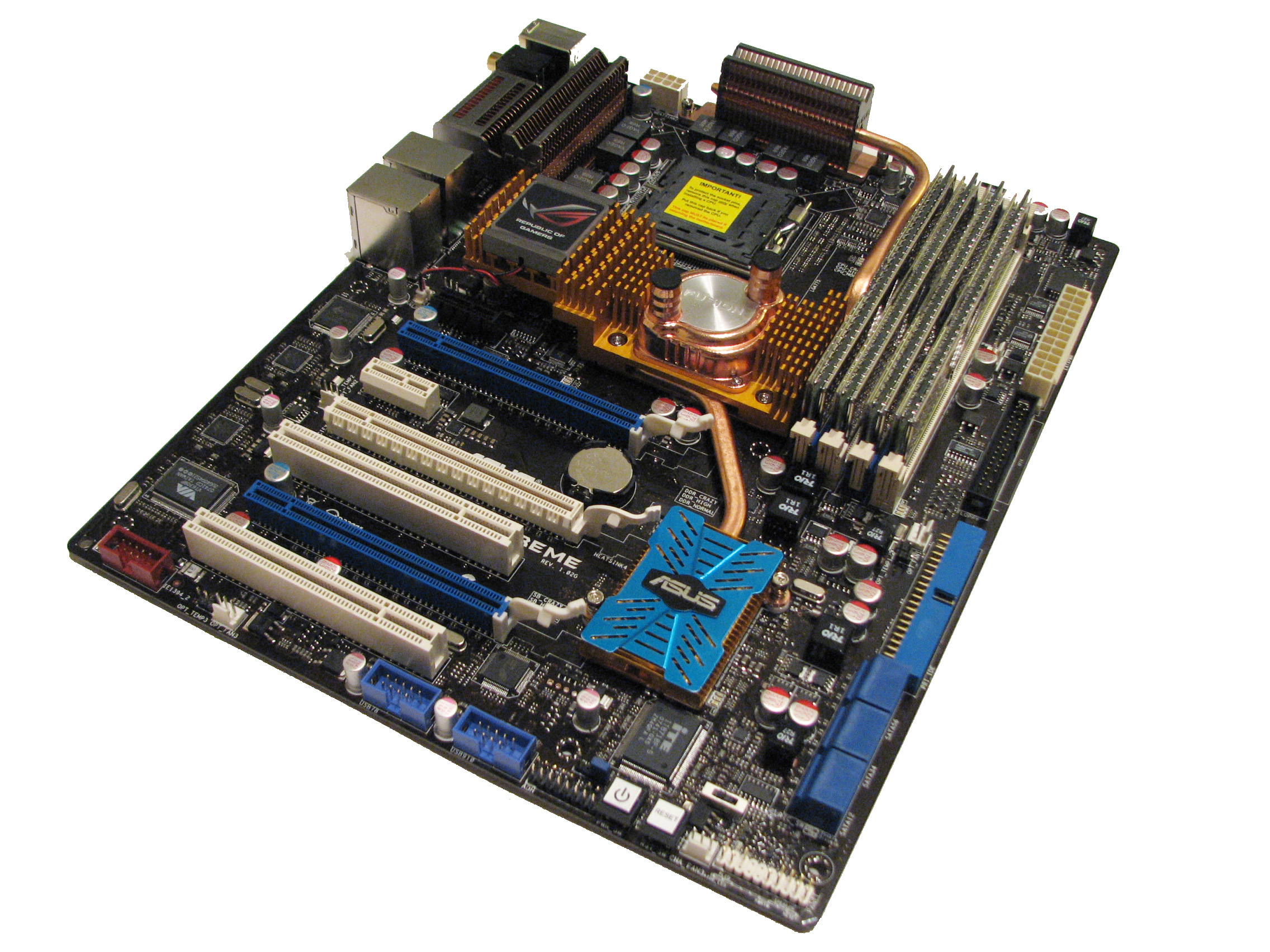
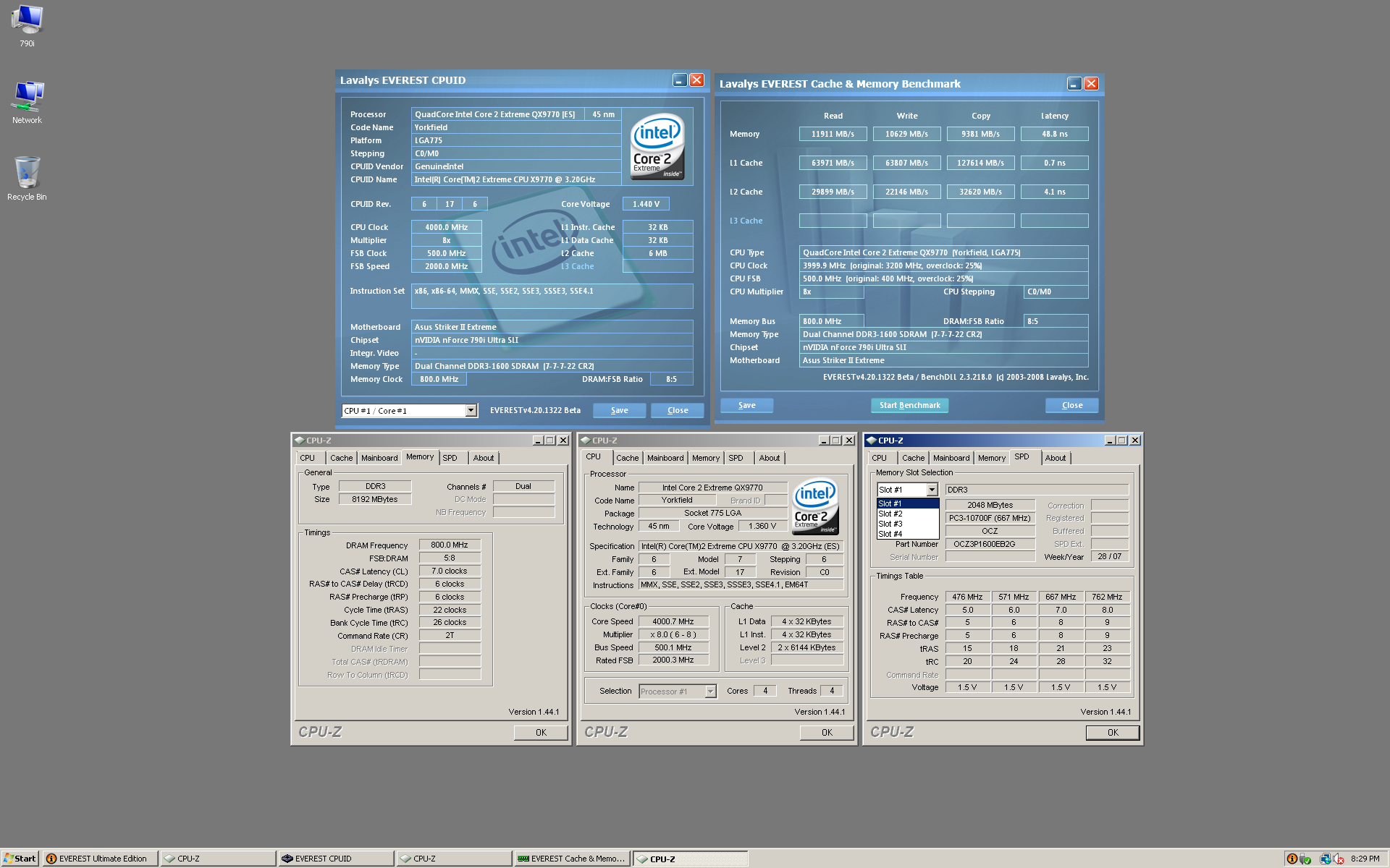
ASUS Striker II Extreme Board Layout and Features
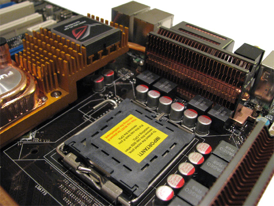
ASUS' third-generation advanced power delivery system is back and as good as ever. ASUS uses the finest ultra-low ESR, polymer capacitors from Fairchild and solid, low-DCR Yageo inductors. Simply noting the inductor count will tell you this board uses an 8-phase PWM, with one small twist though: the PWM buck controller really only supports true 4-phase operation but with an output multiplexer used to double the phase count. This means a sudden power demand placed on the system will only draw current from four of the phases while the other four sit idle, unattached from the load. From this perspective the native 6-phase design used on NVIDIA's reference boards, available from EVGA or XFX, might actually be the better solution.
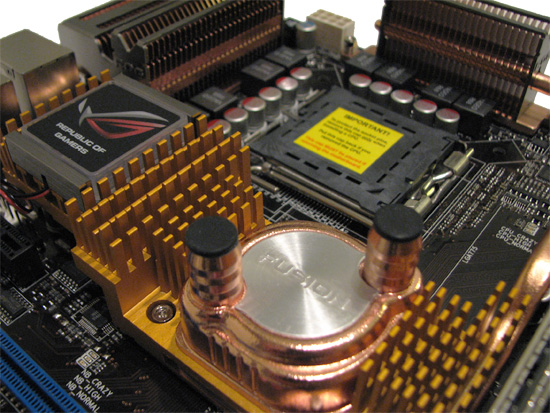
The portion of the heatsink covering the 790i SPP is extruded aluminum with a coating applied to give the illusion of copper. The integrated "Fusion" water-cooling bowl is covered with a thick copper finish inside and out ensuring there will be no issues with galvanic corrosion due to dissimilar metals. The barbs are only 3/8" inner diameter (ID) but a couple of plastic 3/8"-to-1/2" ID straight-through adapters and two 3/8" ID segments of tubing about one-half inch in length are included for those with 1/2" ID water-cooling loops. We found that removing, cleaning, and replacing the factory thermal interface material (TIM) with a small blob of OCZ Freeze was sufficient when it came to cooling the 790i SPP. The included back plates provided all the mounting pressure needed to securely fasten the stock heatsink back in place once we were done with the TIM swap-out.
The backlight for the small Republic of Gamer (R.O.G.) logo attached to the top-half of the heatsink can be turned on or off in the BIOS. Call us crazy but we think building up the fins here, providing more surface area for better heat dissipation seems like a more appropriate use of this precious space. Even a small fan would have been a better choice as far as we are concerned - aesthetics only go so far; every board should be as functional as possible.
The coolers located above each bank of MOSFETs are made of high-quality copper, with an extra segment extending into the area immediately adjacent to the I/O panel. Everything is thermally joined to the SPP heatsink using a closed-loop copper heatpipe and a bit of brazing material. We were pleased to see that ASUS decided to start including back plates for the MOSFET coolers as well. These help to evenly distribute the pressures developed during mounting along the length of the cooler, making certain it sits flush atop the components below.
As with most good DDR3-based designs, the DIMMs are moved slightly down the board bringing them as close to the SPP as physically possible. This can sometimes make things quite cramped when trying to install a longer card in the top PCIe x1 slot. For example, we could not fit our ASUS Xonar D2X sound card in this slot without it contacting the bottom retention key on the closest DIMM slot.
We found configuring our OCZ Platinum DDR3 PC3-14400 memory to run at their full-rated DDR3-1800 speed to be exceptionally simple. What's more, our ASUS Striker II Extreme had no trouble clocking even 8GB of top-end OCZ memory to DDR3-2000 speeds and above - something worth writing home about as far as we are concerned.
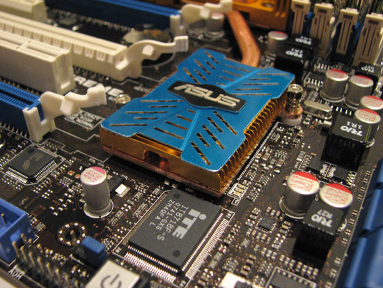
ASUS' MCP cooler is actually quite large - and for good reason, too. The NVIDIA 570i MCP can get very toasty doing a whole lot of nothing. Since it is attached to all the other major heat loads, it is entirely possible we were just seeing the effects of heat transfer from the hotter portions of the heatsink.
If you look closely, you can see the three LEDs located near the bottom-right corner of the cooler. The CPU, SPP, MCP, and memory each have a set of indicator lights - one green, one yellow, and one red - called "Voltminder LEDs". They give the user a quick way of determining roughly how hard each component is pushed. Green signifies that the component is seeing relatively low voltages, yellow warns of increasing stress while red is viewed as a stern warning that damage could occur without the proper precautions (i.e. increased cooling).
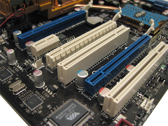
The Striker II Extreme has support for both 3-way SLI and Quad-SLI configurations, in addition to the more traditional 2-way SLI setup. The two blue PCIe x16 slots are PCI Express 2.0 compliant and should be used before a third graphics card is installed in the third white PCIe x16 slot (which is PCI Express 1.x compatible only). You can read more about performance tuning for graphic cards in our included 790i BIOS tuning guide.
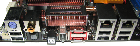
The first PCIe x1 slot (black in color) can be used for either the included SupremeFX II 8-channel HD audio card or any other PCIe x1 device. A second PCIe x1 slot sits directly below the primary graphics slot. A pair of PCI 2.2 slots round out the board's expansion capabilities. Those that rely on wireless networks for connecting to the internet and/or other LAN resources will need to buy a separate wireless adapter as the Striker II Extreme only includes two hardwired RJ45 ports for Ethernet connectivity.
ASUS Striker II Extreme Specifications
| ASUS Striker II Extreme | |
| Market Segment | Ultimate Gamer / Extreme Overclocking - $349.99 (estimated) |
| CPU Interface | Socket T (LGA775) |
| CPU Support | LGA775 Core2 Duo/Extreme/Quad, Pentium EE, Pentium D, Pentium including next-generation 45nm CPU support |
| Chipset | NVIDIA nForce 790i Ultra SLI SPP and MCP (570) |
| CPU Clock Multiplier | 6x ~ 11x, downward adjustable for Core2, upward to 60x for Core2 Extreme, including half-multiplier support for 45nm processors |
| Front Side Bus Speeds | Auto, installed CPU default to 700MHz in 1MHz increments |
| System Bus Speeds | 1600 / 1333 / 1066 / 800 MHz |
| FSB Memory Clock Modes | Auto, Linked, Unlinked |
| DDR3 Memory Ratios | Auto (depends on installed CPU default FSB), 5:4, 3:2 and Sync Mode (2:1) |
| PCIe Speeds | Auto, 100MHz ~ 200MHz in 1MHz
increments PCI 2.0 bus can be adjusted separately from PCI 1.x bus |
| SPP-to-MCP Link Speeds | Auto, 200 ~ 500Mhz in 0.5MHz increments to 210MHz then 1MHz steps |
| HT Multipliers | 1x ~ 5x for SPP->MCP and MCP->SPP |
| EPP 2 Profile Support | Enabled (DDR3-2000 operation), Disabled |
| DRAM Timing Controls | Optimal or Expert (Manual) - tCL, tRCD, tRP, tRAS and CPC |
| Advanced Memory Settings | Auto or Manual - tRRD, tRC, tWR, tWTR, tFAW, tRTP, tRFC and tREF |
| DRAM Command Per Clock | Auto, 1T, 2T |
| MCH P1/P2 Adjustments | Enabled, Disabled |
| CPU Core Control | Enabled, Disabled for each core (excluding Core 0) |
| CPU Voltage | Auto, 1.10000 ~ 2.40000 in 0.00625 increments |
| Loadline Calibration | Enabled, Disabled |
| CPU PLL Voltage | Auto, 1.50V ~ 3.00V in 0.02V increments |
| CPU VTT Voltage | Auto, 1.20V ~ 2.46V in 0.02V increments |
| Memory Voltage | Auto, 1.50V ~ 3.10V in 0.02V increments |
| NB Core Voltage | Auto, 1.30V ~ 2.20V in 0.02V increments |
| SB Core Voltage | Auto, 1.50V ~ 1.85V in 0.05V increments |
| CPU GTLVREF Lane Voltages | Auto, Default, -226mV ~ +224mV for each CPU GTL reference voltage |
| NB GTLREF Lane Voltage | Auto, Default, -126mV ~ +160mV for each CPU GTL reference voltage |
| DDR3 REF Voltages | Auto, Default, -126mV ~ +160mV for each DDR3 channel |
| Memory Slots | Four 240-pin DDR3 DIMM Slots Dual-Channel Memory Architecture Regular Unbuffered, non-ECC DDR3 Memory to DDR3-1333, 8GB Total Supports SLI-Ready EPP 2 Memory to DDR3-2000 |
| Expansion Slots | 2 - PCIe 2.0 x16, supports NVIDIA SLI and Quad-SLI
Technology 1 - PCIe (1.x) x16, allows NVIDIA 3-way SLI with 8800GTX/Ultra 2 - PCIe (1.x) x1, one compatable with audio solution 2 - PCI Slot 2.2 |
| Onboard SATA RAID | 6x SATA 3.0Gbps Ports - nForce MCP (NVIDIA MediaShield RAID 0, 1, 0+1, 5 and JBOD) |
| Onboard IDE/Additional SATA | Jmicron JMB363 SATA Controller (2 external eSATA ports) |
| Onboard USB 2.0/IEEE-1394 | 10 USB 2.0 Ports - (6) I/O Panel, (4) via
headers 2x 1394a Ports - (1) I/O Panel, (1) via header |
| Onboard LAN (with Teaming) | Dual NVIDIA nForce LAN with DualNet and FirstPacket Technology |
| Onboard Audio | 8-channel HD Audio (Azalia) CODEC |
| Power Connectors | ATX 24-pin, 8-pin EATX 12V |
| I/O Panel | 1 x PS/2 Keyboard 2 x SPDIF - (1) Optical Out, (1) Coaxial Out 2 x External eSATA 1 x IEEE-1394a port 2 x RJ-45 (LAN) 6 x USB 2.0 CMOS Reset Button 8 Channel Audio I/O (optional included SupremeFX II Audio Card) |
| Fan Headers | 8 - (1) CPU, (1) Power, (6) Chassis |
| BIOS Revision | 0511 |
Because all 790i (Ultra) boards employ a BIOS based on reference NVIDIA code, we were not surprised to note the many similarities between the ASUS Striker II Extreme and the EVGA 790i offering reviewed at product launch. The Striker II Extreme mostly expands upon the already generous voltage ranges, providing many well beyond the realm of sanity, as well as a couple other switches some may find practical.
Regardless of how you feel about subjecting your 45nm processor to exceedingly high voltages - up to 2.4V minus a nominal droop is possible with this board - more than a few onboard components as well as installed DDR3 memory modules will be damaged if you test the upper limits of each range. To make safeguarding your investments easier we have created this simple to follow voltage limit reference when it comes to overclocking the 790i MCP and a 45nm CPU. Our maximum recommended values are based on safe, reliable, sustained 24/7 operation of each component using either conventional air-cooling or more efficient water-cooling.
Those that plan to pair an older 65nm processor with their 790i motherboard may have a little more margin when it comes to the application of higher CPU core voltages; in this case we would recommend no more than 1.55V. Moreover, the limits listed should be read as maximum in-BIOS selections as these values already take into account any droop in actual voltages. Finally, as a general disclaimer, it is important to recognize that overclocking can subject components to additional stresses that may result in damage, degradation in performance, or even premature failure.
| Voltage Limits | |||
| Highest Voltage Setting Available in BIOS |
Maximum Recommended for Sustained Operation |
Near Instant Damage Occurs at... |
|
| CPU Voltage | 2.40V | 1.50V | 1.80V |
| CPU PLL Voltage | 3.00V | 1.60V | 2.00V |
| CPU VTT Voltage | 2.46V | 1.36V | 2.00V |
| Memory Voltage | 3.10V | 2.00V | 2.40V |
| NB Core Voltage | 2.20V | 1.60V | 2.00V |
| SB Core Voltage | 1.85V | 1.60V | n/a |
Worth noting is that our board disallowed any FSB lower than the installed CPU's default value - a rather odd precept when it comes to overclocking. We would like to see this changed though as there is no obvious benefit to this policy (it only serves to hamper troubleshooting efforts with problems possibly related to higher bus speeds). The Striker II Extreme permits FSB speeds as high as 700MHz, which is more than enough headroom for even extreme overclocking. Reaching such high FSBs is a different story, of course.
Nearly the same as the 790i reference board, PCIe bus interfaces associated with the SPP and MCP can be overclocked separate from one another. Slot 1 and 2 PCIe link resources are provided by the 790i SPP, a PCI Express 2.0 capable part, while Slot 3 hangs off the 570 MCP and conforms to PCI Express 1.x specifications only. The difference is that with the Striker II Extreme, unlike the NVIDIA reference design, PCIe Slot 1 and 2 each receive their master clocking signal from the same physical PLL instead of separate circuits with individual oscillators.
Although we're not absolutely certain, this is perhaps the reason why we were utterly unsuccessful in overclocking the PCIe 2.0 interface with our Striker II Extreme, while the reference design sailed well past 150MHz with relative ease. This was disappointing as earlier testing with the EVGA 790i-based board showed significant 3D performance gains (up to 10%) attributable to this change alone.
Another major drawback with the platform as a whole is the incorporation of an MCP absent a PCIe 2.0 interface, an issue we have been critical of with Intel in the past. Intel's decision to release their X48 Express chipset prior to the availability of their new ICH10(R) Southbridge undoubtedly allowed NVIDIA the opportunity to forgo the design and production of a competitive MCP - making us the real losers in the end.
This may be one of the reasons 3-way SLI shows only moderate gains over traditional 2-way configurations. The addition of a third graphics card theoretically enhances a system's ability to handle larger 3D workloads (provided the CPU power is there), but in most circumstances data transfer constraints imposed by the slower SPP-to-MCP PCIe link inhibit the effective employment of all available GPU resources. It is probably unfair to point finger at Intel for the lack of innovation in NVIDIA products, but it is not far from the truth. When it comes to desktop chipsets, most of the time NVIDIA is simply struggling to keep up with Intel.
Test System Configuration and Methodology
| Test System Configurations | |
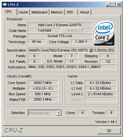
| Processor(s) | Intel Core 2 Duo E8500 (ES) Dual-core, 3.16GHz, 6MB Unified L2 Cache, 9.5x Multiplier, 1333 FSB Intel Core 2 Extreme QX9770 (ES) Quad-core, 3.20GHz, 2x6MB Unified L2 Cache, 8.0x Multiplier, 1600 FSB |
| Motherboard(s) | ASUS Striker II Extreme (NVIDIA 790i Ultra SPP and
MCP) EVGA NVIDIA nForce 790i Ultra SLI (NVIDIA 790i Ultra SPP and MCP) EVGA NVIDIA nForce 780i SLI (NVIDIA 780i SPP and MCP, nForce 200) MSI PN7 SLI Platinum (NVIDIA 750i SPP and 480 MCP) ASUS P5E3 Premium (Intel X48 Experss MCH and ICH9R) |
| DDR2 Memory | 2x1GB Crucial Ballistix PC2 8500 (DDR2-1066) |
| DDR3 Memory | 2x1GB Crucial Ballistix PC3 12800 (DDR3-1600) |
| Graphics Card(s) | MSI 8800 GTS 512MB (G92) - single and SLI
configurations 675MHz core, 1625MHz shader, 970MHz (DDR-1940) memory |
| Cooling | D-tek FuZion CPU block, EK-FC88 GT/GTS full coverage GPU blocks, ThermoChill PA120.3 radiator, 3x SUNON KDE1212PMB3-6A 120x38mm fans, Laing D5 pump, 1/2" ID (3/4" OD) Tygon tubing |
| Power Supply | OCZ EvoStream 600W Modular PSU |
| Hard Drive | WD 74GB Raptor, 10K RPM, SATA 3Gbps, 8MB buffer |
| Video Driver | NVIDIA 169.25 (WHQL) |
| Operating System | Windows Vista Ultimate (x64) SP1 with DirectX 10.1 |
Each motherboard was flashed with the latest available BIOS - some of which were still labeled beta at the time of testing - and any unneeded functionality was disabled (unused serial ports, onboard HD audio, IDE controllers, etc.). This streamlined the OS and driver installs for optimum performance.
Prior to each round of motherboard testing we loaded a fresh install of Windows Vista Ultimate (x64), followed by platform drivers, then Service Pack 1 (SP1) including all patches and hot fixes currently offered by Microsoft's online Windows Update service. We made sure that our hard disk's write-back caching was enabled and the prefetch folder was cleared before each test run.
The latest WHQL-certified video drivers for our pair of MSI 8800GTS 512MB (G92) cards were then installed and all NVIDIA control panel settings were left as-is with the exception of SLI functionality, which was selectively enabled and disabled depending on which round of benchmarks were being run. Additionally, rather than deal with comparison issues arising from GPU core, shader, and memory clocks speed discrepancies seen from card to card, depending on the vendor, we chose to flash our pair of graphics cards to the NVIDIA reference clocks as listed on their site. Therefore, if some of our scores seem low to you it may be because the cards you have been working with come factory-programmed with higher clock frequencies.
Our test suite consists of Futuremark 3DMark 2006, a popular 3D benching program, Futuremark PCMark Vantage (x64), Crysis (32-bit executable), Unreal Tournament 3, Company of Heroes: Opposing Fronts, and Lavalys' EVEREST Cache and Memory Benchmark tool. All game benchmarks are run at a higher resolution (1920x1200) and a lower resolution (1280x1024), always on "High Quality" settings - with the exception of Crysis that was run at "Medium" settings - and in each case results are reported with and without SLI enabled, whenever possible. In addition, these tests used our Core 2 Duo E8500 dual-core CPU as well as our quad-core QX9770. Finally, we show scores at both stock processor frequencies and rated bus speeds and when overclocked to 4.00GHz (8x500MHz for the E8500 and 10x400MHz for the QX9970).
We ran each test five times, threw out the high and the low score, and then averaged the remaining three. These results fully qualify the advantages (or not) of purchasing a more powerful CPU - whether that means higher frequencies or more cores - along with any real-world benefits of NVIDIA's SLI Technology.
There is one exception to this: the ASUS P5E3 Premium. Although a worthy contender, the P5E3 Premium is not SLI-capable due to drivers, and as such we do not provide SLI results. Future testing using Crossfire-capable ATI/AMD HD 3800-series cards will be completed in the next roundup, but for now we're concentrating on SLI. We've really added the P5E3 Premium to the mix just to get a feel for how X48 stacks-up against NVIDIA's 750i, 780i and 790i Ultra when it comes to single-card graphics performance. This will be good information for those that are not necessarily in the market for an SLI-capable motherboard or feel gaming may not be their top priority.
Before we get into the specifics let's look at overall system performance. We chose PCMark Vantage for this task as it does an excellent job of documenting the performance of nearly every subsystem and then combines the results in a meaningful way. This allows us to conduct a broad sweeping check of the system as a whole; then, if the score is unusually low, we can decide whether investigation and further testing may be prudent.
Overall System Performance with PCMark Vantage
Futuremark claims PCMark Vantage for Vista is the most complete total system-benchmarking suite to date and our experience has shown this to be true. The benchmarks are designed to test the performance of each major subsystem - CPU, memory, graphics, and disk performance based on real world applications. The final score presented at the conclusion of each test run takes into account the results of each carefully tailored test within the benchmark suite.
Because our goal was the measurement and analysis of motherboard performance, we took great care to use equivalent parts whenever possible. As such, each test setup utilized the same exact hard disk drive model, graphics card(s), and installed processors. The only real difference worth nothing is the memory and the chipset installed on each board. We used different modules depending on whether the motherboard tested used DDR2 or DDR3 memory. We used memory from the same manufacturer (and product line) in order to nullify any potential advantage arising from the use of dissimilar components.
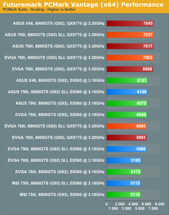
As we can see, DDR3 motherboards based on NVIDIA 790i or Intel X48 chipsets score well above those that use DDR2 modules. Clearly, the additional memory read bandwidth and reduced access latencies associated with the faster DDR3 subsystems have a distinct affect on overall system performance. This is worth keeping in mind when it comes to buying your next motherboard - DDR3 prices continue to fall every day and we would argue that these once overly expensive products are now almost within the realm of affordability.
Switching from an E8500 dual-core CPU to a QX9770 quad-core provided an additional performance boost to the tune of about 1000 points on average. The fact that subsystem scores are additive in nature is demonstrated well by the EVGA 780i results - in this case, this same 1000-point increase can be seen, regardless of the initial lower score when compared to the other systems that managed to score higher overall.
Finally, PCMark Vantage measured absolutely no performance advantage when enabling NVIDIA's SLI Technology. Although the benchmark does run a couple of graphics-intensive tests, they are conducted in windowed mode and do not appear to respond to the additional available graphics horsepower provided by multi-GPU configurations.
We can conclude that the scores achieved by each system were a result of the components in use, and had nearly nothing to do with the actual motherboards utilized. That is to say, the motherboard merely functions as a platform for the installation of the components and has little to do with the development of actual performance; rather it simply allows the installed components to reach their full potential.
What this really means is that users who plan to run their systems in stock configurations will have a hard time going wrong with any motherboard examined above (and quite possibly any motherboard based on any of these four chipsets or others). The qualities and individual benefits of each motherboard do not become fully evident until overclocking comes into play. Let's move on to synthetic graphics performance courtesy of 3DMark06.
Synthetic 3D Graphics Results
Futuremark's 3DMark06 benchmark scores depend solely on two subsystem evaluations: how powerful is your 3D graphics card(s) and just how good is your CPU at crunching numbers? In fact, memory bandwidth and access latencies have no noticeable effect on the final score. Of course, there are games that also show little benefit from improvements in the memory subsystem. Regardless, 3DMark06 is and always will be a synthetic benchmark and we put more stock in actual gaming performance results.
It is good for one thing though - it gives us a good idea of the gains made possible by installing a second, or even third or fourth GPU. However, this is not always the case as some games respond rather dismally to the addition of a second GPU while others may experience the nearly full theoretical performance increase (double the frame rate at an equivalent resolution).
What it really comes down to is how well the game has been engineered from the start to effectively distribute the graphics load across all available GPU resources. Yet another consideration in all of this is the level of success shared by the graphics drivers and platform solution in efficiently routing data between individual subsystems as needed to drive higher frame rates. Of course, the amount of CPU processing power available plays a role and as we will see, more capable processors sometimes allow SLI to offer additional scaling above what would be possible with a lesser CPU.
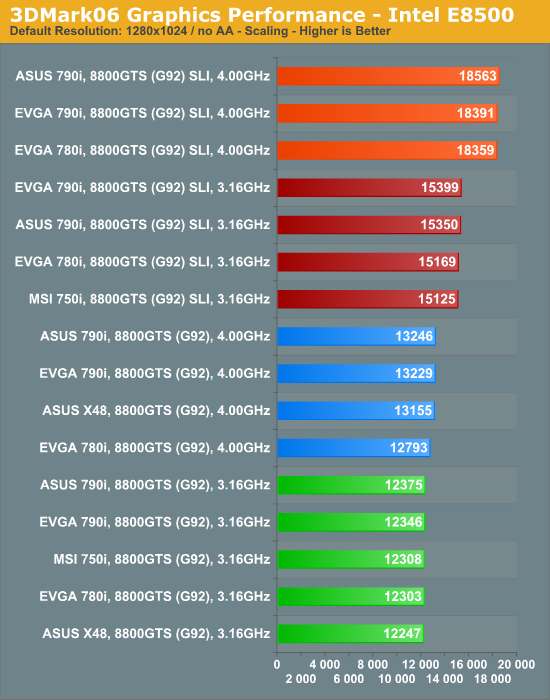
First out of the gate is our 45nm Intel E8500 dual-core CPU. Simply overclocking the processor to 4.00Ghz (8x500MHz), up from the default 3.16GHz frequency, produces only mild gains as measured by 3DMark06 - about 7% due entirely to the improved CPU test sub-score.
Adding a second GPU is an entirely different matter though - one in which graphics performance becomes linked with general processing power. Case in point: adding a second 8800GTS 512MB (G92) graphics card to our Striker II Extreme with the E8500 at default speeds result in about a 25% increase in 3DMarks (15,350 up from 12,375) while doing the same with the CPU overclocked to 4.00GHz shows over a 40% increase in 3DMarks (13,246 to 18,563).
Certainly, a portion of this gain can be attributed to the higher CPU speed, but the question then becomes, what percentage of the increase can be credited to improved SLI scaling? A quick calculation uncovers that had the scores at 4.00GHz with SLI not benefitted from the higher CPU sub-score it still would have beaten out the 15,350 3DMarks (E8500 at stock with SLI) by a healthy 12.2% with a score somewhere in the neighborhood of 17,222 3DMarks. Not only did a ~26.5% increase in CPU frequency result in a better CPU test sub-score but general graphics performance improved as well.
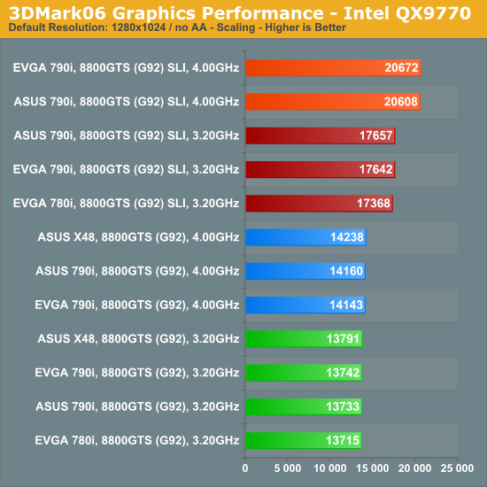
Our field of players for the quad-core tests is a little smaller due to a number of reasons - the first being our utter failure in getting the 45nm Intel QX9770 to boot Vista on the MSI PN7 SLI Platinum. (Seeing as this board uses the 750i chipset, this did not come as a surprise.) Secondly, our EVGA 780i board refused to play nice at the higher 4.00GHz clocks speed with a quad-core.
Both the EVGA reference 790i board and the ASUS Striker II Extreme easily eclipsed 20K 3DMarks on 3DMark06 with the QX9770 overclocked to a stable 4.00GHz and two 8800GTS 512MB (G92) cards in SLI. As we mentioned earlier, our graphics cards run at NVIDIA-specified stock clock speeds - even higher scores are possible using some vendors' "superclocked" models (or via user GPU overclocking). As we can see though, a 50% increase in 3DMarks can be achieved by simply installing a second graphics card and subsequently overclocking the QX9770 to 4.00GHz.
Game Testing - Crysis
A favorite action title among today's gamers is without a doubt Crysis from EA Games. The trouble is that building or buying a system capable of running Crysis at acceptable frame rates using higher resolutions with all the eye candy turned on is next to impossible. SLI scaling, and Crysis performance in general, has improved lately, thanks to a few of the more recent non-WHQL ForceWare driver releases from NVIDIA, but it's still not quite up to speed as far we're concerned. Perhaps the next generation of GPUs will address this problem head-on.
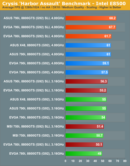
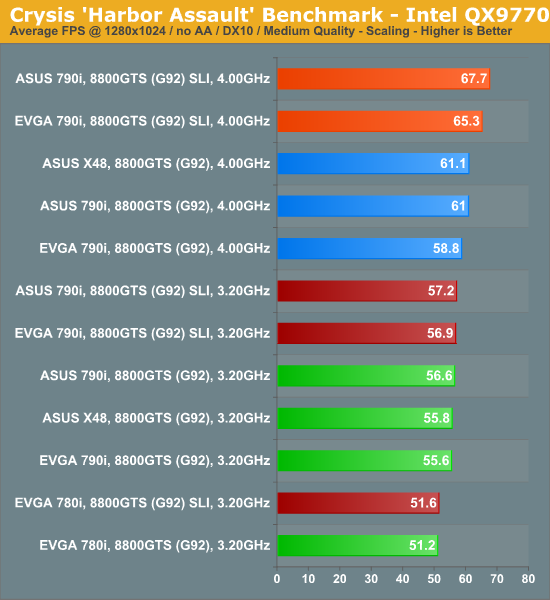
Assuming you game at 1280x1024, an Intel E8500 and even a single 8800GTS 512MB (G92) graphics card is more than capable of rendering Crysis at average frame rates around 50FPS and above. Unfortunately, gaming at this lower resolution is not always the norm and certainly leaves much to be desired when compared to the amazing image displayed on a larger 24" flat panel LCD.
This round of results seems to suggest that Crysis is somewhat sensitive to memory performance and memory access latencies, at least at lower resolutions. The EVGA 780i reference board and MSI PN7 SLI Platinum, both of which use DDR2, trail all other DDR3 boards, even with SLI enabled. We considered the possibility that the older PCI-e 1.x technology used on these boards was the bottleneck (remember, 780i's PCI-e 2.0 support comes from a non-native bridge chip) but quickly dismissed this idea - it is far more probable that either the CPU or the memory subsystems are the limiting factors, especially at this low resolution.
Interesting to note is that if you do plan to play Crysis at this lower resolution you may be better off overclocking your CPU than buying a second graphics card, given the choice between the two. Even better, spend the money you set aside for that second graphics card on a new 790i or X48 motherboard - our test results show these two top-end chipsets (using DDR3) in single-card configurations keeping up with 780i with two graphics cards in SLI. Of course, if you already own a 780i-based motherboard chances are you are running SLI already. In that case moving up to a 790i-based motherboard will net you 15% higher frame rates using today's latest WHQL-approved ForceWare drivers.
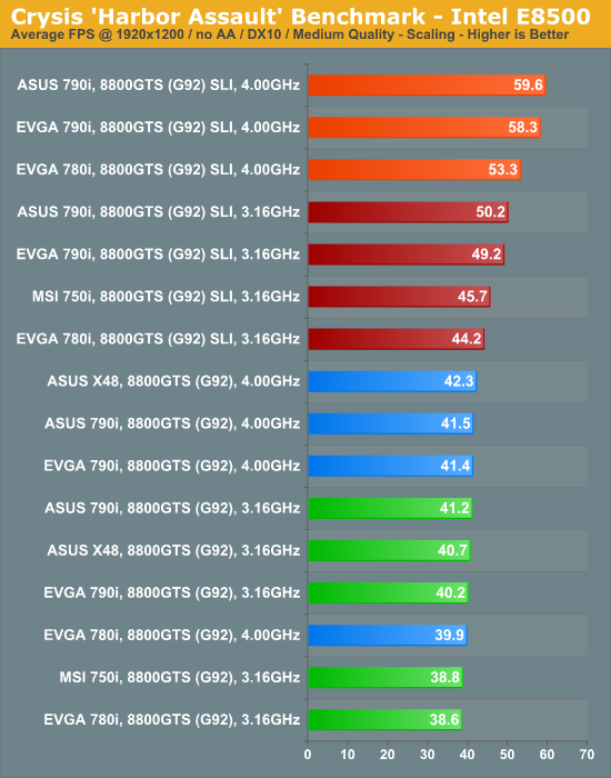
Performance scaling with Crysis at 1920x1200 is an entirely different ballgame - the bottleneck is no longer the CPU and memory subsystems as evident by the non-existent frame rate improvements when overclocking our E8500 from the stock 3.16GHz to 4.00GHz. In fact, SLI does little to help the situation when installed in 750i- or 780i-based motherboards. The EVGA reference 790i board and the ASUS Striker II Extreme demonstrate they are more than capable of handling the load when configured properly.
Even with the additional processing power provided by two more cores, the EVGA 780i trails all others when it comes to average frame rate. This is more evidence that tends to support our earlier assumption that Crysis is sensitive to memory bandwidth at lower resolutions. Moreover, the lack of improvement when compared to the dual-core results above clearly indicates that Crysis is unwilling to make efficient use of more than two cores. If playing this game is the purpose of your next build your money will be better spent on motherboard and DDR3 memory upgrades rather than the latest quad-core CPU.
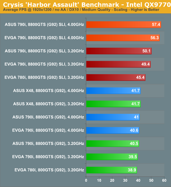
Once again, our scores are limited by our graphics capabilities. The only thing that is going to improve these frame rates at this point is more powerful GPUs. Assuming Quad-SLI is optimized for this game, two 9800GX2 cards may provide us with the means to push nearly 60FPS on "High" settings - quite an achievement considering the ability of DirectX 10 shaders to bring nearly any graphics card to its knees.
Game Testing - Unreal Tournament 3
Unreal Tournament 3 (UT3) continues to be one of our favorite games and as such tends to be one of the more scrutinized titles when it comes to graphics performance. This fast-action first-person shooter demands high frame rates if you are to be successful playing against others online. The slightest bit of lag or the occasional jerky picture response can quickly degrade the game playing experience to the point of absolute frustration. UT3 also happens to be quite demanding when it comes to CPU performance.
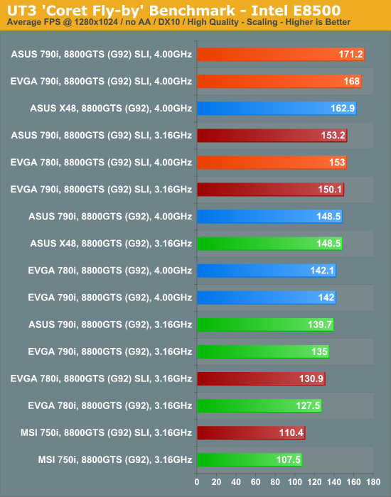
Much like Crysis, UT3 frame rates at lower resolutions will suffer with slower memory subsystems. We have found UT3 to be very latency sensitive, which is one of the reasons why the Intel X48 chipset stands out so well at 1280x1024.
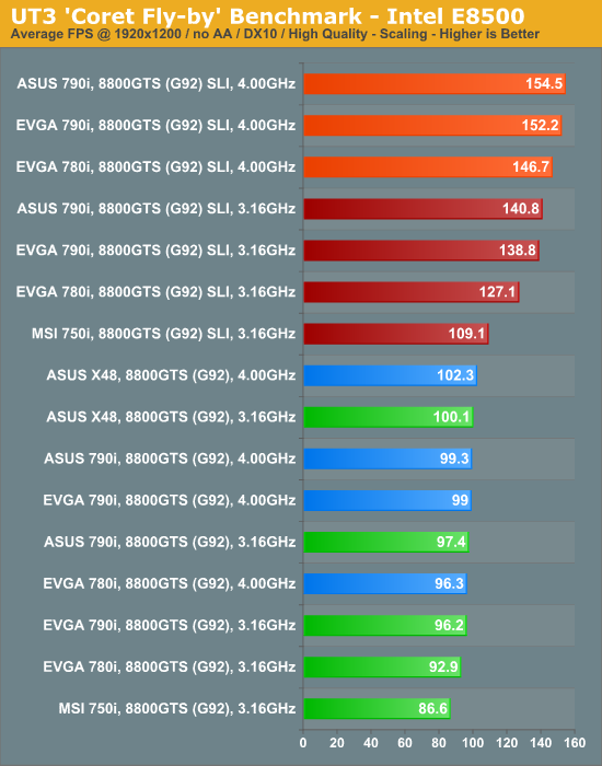
By moving to the higher 1920x1200 resolution, we can see exactly where the graphic system becomes the bottleneck and limits the average frame rate to about 100FPS regardless of CPU speed. As we have seen before, the 750i and 780i fall behind in SLI, with as much as a 50% performance improvement to be had when moving up to 790i. At these frame rates though, this extra performance margin would be much better put to use with 4xAA/16x AF turned on.

Unlike Crysis, UT3 benefits from the use of our QX9770, more so without SLI than with. The ever-ensuing tradeoff between which subsystem becomes the performance limiter should stick out as a common theme by now. Discounting SLI configurations, Intel's X48 holds the lead here due to the reduced memory latencies experienced with this chipset.
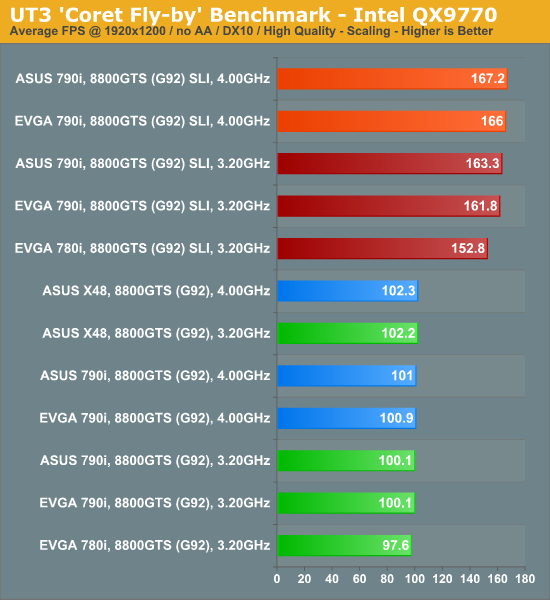
At higher resolutions, UT3 does benefit from the QX9770 CPU, but not because of what you might think. Improved SLI scaling due to the abundance of processing power allows for slightly better average frame rates when using more than one GPU. The lower cap at around 100FPS is still present with the single-GPU configurations. If we were going to build a SLI system for playing UT3, it would be with the goal of running high AA/AF levels at a resolution of 1920x1200.
Game Testing - Company of Heroes: Opposing Fronts
Company of Heroes: Opposing Fronts arrived last year and remains one of the best samples of the genre we have ever played. We find the game to be extremely GPU intensive and a hefty CPU is definitely required as well. This title contains a built-in performance test that makes use of the game engine, generating several different scenes representative of the in-game experience, which we believe provides a very good indication of just how well the system will perform during actual play. We use the DX9 rendering engine for testing purposes as the DX10 code path can quickly bring even the fastest system to its knees.
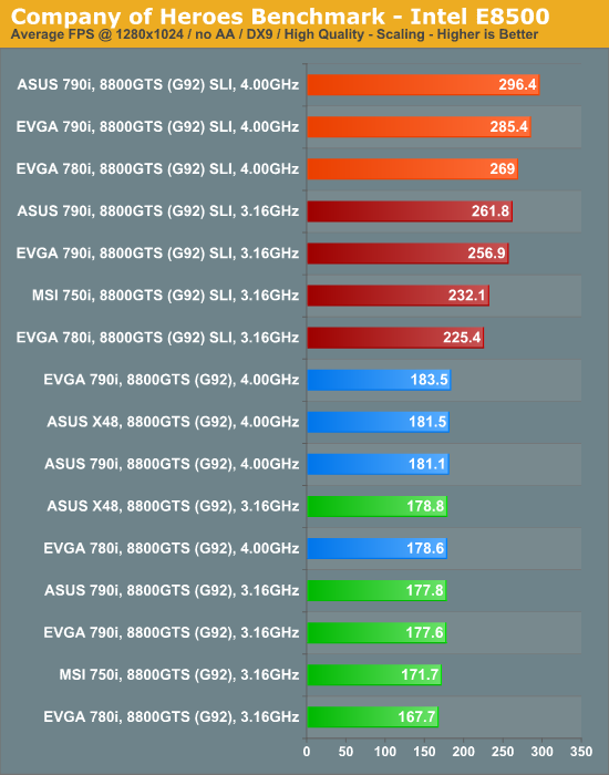
Unlike some other titles we have tested, Company of Heroes shows signs of being GPU-limited at lower resolutions (1280x1024) where the CPU is usually the bottleneck. Increasing our E8500's frequency alone from 3.16GHz to 4.00GHz did little to improve frame rates. The game did however exhibit excellent performance scaling with the use of two 8800GTS 512MB (G92) graphics cards in SLI. Once again, the two newest 790i boards had no trouble distinguishing themselves from the pack, outscoring the 780i- and 750i-based boards clock-for-clock by as much as 10%.
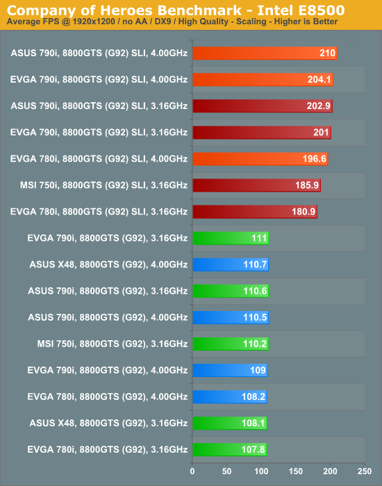
Moving to the higher 1920x1200 resolution undeniably places a larger share of the performance burden on the graphics subsystem. While average frame rates do decrease, scaling with SLI enabled comes very close to the magical, theoretically maximum of a full 2x increase in performance.

Even our quad-core QX9770 showed gains with Company of Heroes, demonstrating why this gaming engine deserves all the praise we can muster. The two 790i-based motherboards continue to hold a solid 10% lead over the similarly configured 780i board as well. In fact, the EVGA 780i board is unable compete at the highest 4.0GHz overclock - we just could not manage to keep the board stable long enough to complete the benchmark.

At 1920x1200, the quad-core results closely resemble those taken from the dual-core testing, which supports our earlier statements regarding the heavy GPU limitations at this resolution.
Intel 45nm Quad-Core Overclocking
Perhaps the greatest ability the ASUS Striker II Extreme has to offer is its amazing performance when overclocking 45nm dual-cores, 45nm quad-cores, and high-speed DDR3 memory. We have tested numerous motherboards built on many different platforms with several different chipsets but none has performed as well as the ASUS Striker II Extreme when it comes to overclocking our Intel QX9770. A little time spent with tweaking the GTL reference voltages and we found ourselves starting at a Prime95 stable system running a 45nm quad-core at 500MHz FSB.
 A 45nm quad-core at 500MHz FSB? Doth my eyes deceive me? |
We then turned our sights to memory overclocking and decided to see just how far we could push 8GB of OCZ DDR PC3-14400 Platinum Edition memory. One of the secrets to running high physical memory densities - whether DDR2 or DDR3 - is tRFC, an important memory timing parameter, necessary for the proper refresh of SDRAM circuitry. Although JEDEC provides different tRFC minimum value specifications for each device density, most overclockers ignore these values when it comes to achieving maximum system performance.
 While DDR3-2000 memory speeds may no longer be impressive to some, we tend to believe seeing this with 8GB of DDR3 is quite an accomplishment for today's boards. |
Because of the design of memory, SDRAM must be periodically refreshed in order to retain the validity of data stored in each memory cell. All banks of the SDRAM must be precharged and idle for a minimum of the Precharge Time (tRP) before this refresh command can be applied. Once the refresh cycle has completed all banks of the SDRAM will then be in the precharged (idle) state and a delay between the Refresh Command and the next Active Command or subsequent Refresh Command must be greater than or equal to the Refresh Cycle Time (tRFC).
Higher memory device densities with a greater number of SDRAM banks require more cycles to complete this refresh sequence. The number of clock cycles needed to satisfy the tRFC minimum specification for a system configuration consisting of a pair of 2GB modules, although not double that of 1GB modules, is still significantly higher - about 53% higher according to JEDEC figures - and installing four separate modules in place of two makes consideration of this timing even more critical.
 This is just the level of performance we have come to expect from DDR3. The fact that we can achieve this with 8GB though is simply awesome. |
Our greatest memory performance point actually came at DDR3-1600 (500MHz FSB and a 5:4 divider) with 8GB of memory. We could not get the system to run without errors with 8GB at DDR3-2000 with "P1" and "P2" enabled (we will talk more about these particular settings later in the BIOS guide). Backing down to DDR3-1600 and enabling these values boosted our memory read scores to almost 12GB/s.
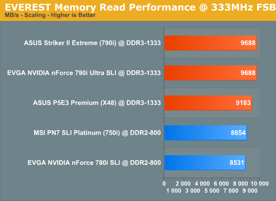
Memory Access Latency and Read Performance
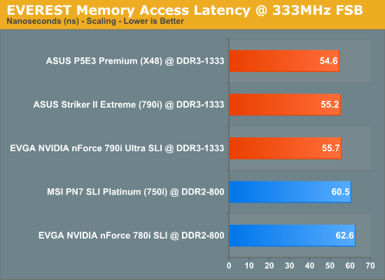
Each of the DDR3-based motherboard showed about a 10% reduction in random memory access latency figures. As expected, the board with the Intel X48 Express chipset, the ASUS P5E3 Premium, takes the gold in this event.
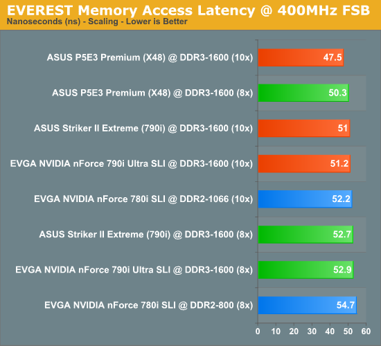
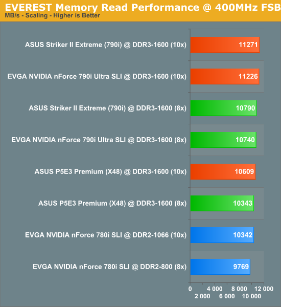
400MHz FSB showed additional small improvements with even lower memory access latencies. Unlike the boards with an NVIDIA chipset, the ASUS P5E3 Premium showed another nice drop in latency simply by moving to the higher multiplier (overclocking our QX9770 from 3.20GHz to 4.00GHz). As previously noted, these low access times are precisely the reason why UT3 runs so well on our X48 board.
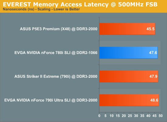
We saw the best memory access latencies of the day with our X48-based P5E3 Premium at 500FSB. The real surprise however came from the EVGA NVIDIA nForce 780i SLI, which showed DDR2 could be nearly as effective at producing low access times as DDR3 when properly tuned.
NVIDIA really surprised us with the quality of their first DDR3 memory controller; besting Intel's X48 design was the last thing we expected to see from 790i. According to these results, even DDR3 value memory outperforms the midrange DDR2 modules flooding the market.
Both EVGA's and ASUS' 790i boards absolutely demolished the P5E3 Premium when it came to raw memory read bandwidth - 500MB/s is a big lead to hold when comparing memory controller performance with memory running at equivalent speeds. The extra 10% memory read throughput seen with DDR3-1600 over DDR2-1066 shows up well in some of the gaming benchmarks. This goes a long way towards dispelling the early, unsubstantiated rumors of lackluster performance from DDR3 memory.
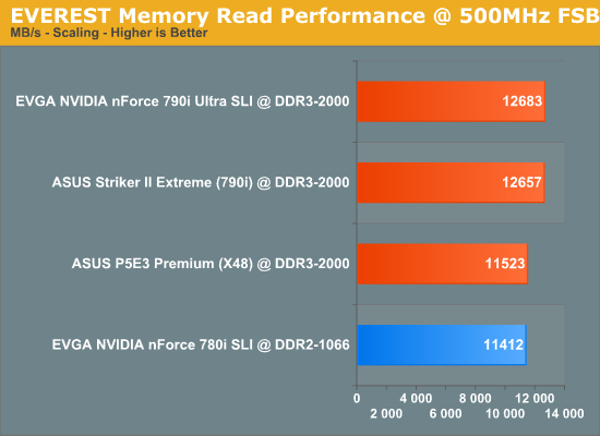
The 790i pulls even farther ahead when the FSB is increased to 500MHz. Intel's X48 Express chipset begins to run out of steam at around 465-475MHz FSB. The same would be true for NVIDIA's 790i Ultra if it were not for the cryptic "P1" and "P2" BIOS options.
Memory Write and Copy Performance
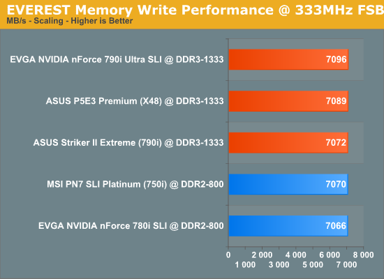
Memory write performance is almost solely dependent on FSB, although changes in absolute CAS latency can have a much smaller secondary affect. There is no clock crossing procedure needed when moving data across the FSB onto the memory bus during write operations; therefore total memory throughput is based largely on the speed of the interface and nothing more. DDR3 shows improvements over DDR2 in this regard.
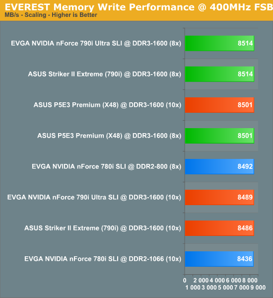
The trend carries on through 400MHz FSB where a 20% increase in FSB leads to an equivalent 20% increase in memory write performance.
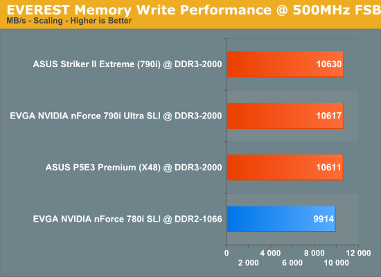
Each of the DDR3 boards continues scaling to 500MHz FSB with the expected 25% jump in memory write performance over 400MHz FSB. However, the DDR2-based 780i board stalled at just under 10GB/s signifying a rather serious problem with memory writes with this board. Whatever the problem was NVIDIA has obviously implemented the fix in 790i.
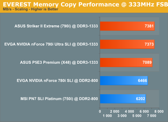
Memory copy benchmarks are unique in that they provide a great indication of just how well a memory controller balances the importance of read versus write requests. A chipset certainly cannot facilitate good copy speeds if read or write performance is low. The memory controller must first read the data from memory before it can write it back to memory (this is basis of a copy operation) and a bottleneck with either can bring everything to a crawl. Naturally, the DDR3 boards have an advantage in read performance at equivalent clock speeds and easily outclass the DDR2 boards.
To our surprise memory copy performance sometimes actually exceeded memory write speeds for the same FSB - in this case the 790i showed unexpected efficiency. A possible explanation for this phenomenon is the manner in which memory write requests are sometimes internally queued by the MCH until a lapse in memory read requests provides opportunity for a quick burst of write data to be sent across the memory bus, unimpeded by competing traffic.
In this respect, bandwidth as measured from the viewpoint of total memory throughput would be higher. Although the time to complete the pending write request might suffer, most writes are highly asynchronous - there would be little need for an instantaneous write operation unless an immediate read request depended on data stored by the same write to memory. In that case the controller could recognize this condition and simply read the data from the "cache line" without even touching main memory. You could almost argue that the MCH provided the functionality indicative of a highly specialized L3 cache in this particular situation.

We see here the roles reversed with the X48 Express chipset showing better memory copy performance than both 790i-based boards.
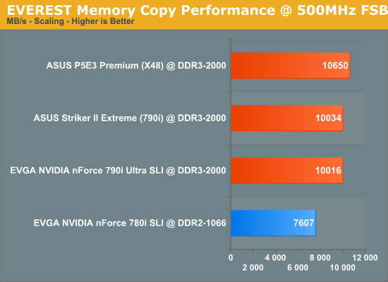
The Intel X48 Express wins again at 500MHz FSB, an oddity considering the commanding lead held by 790i when it comes to memory read performance at this system bus speed. We are tempted to give Intel's X48 the nod for the win, seeing as how it either wins or ties 790i in three out of four tests (memory access latency, memory write performance, and memory copy performance).
Complete BIOS Tuning Guide - "Extreme Tweaker"
This guide's intent is to help those with limited overclocking experience or those unfamiliar with NVIDIA-based motherboards in learning the basics when it comes to overclocking DDR3 memory using the 790i MCP. All of these options can be directly accessed from the main BIOS setup page entitled "Extreme Tweaker" or from one of the four submenus listed below.
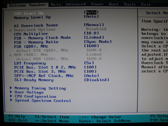
Extreme Tweaker
CPU Level Up - [Auto, Crazy] Selecting Auto, our recommended setting, allows for user adjustments of each individual CPU and memory overclock option (when available). If anything other than Auto is used the only overclocking option that can be manipulated is CPU Multiplier.
Crazy automatically sets AI Overclock Tuner to CPU Level Up, locks the FSB to the next higher tier based on the installed CPU's default value (333MHz goes to 400MHz, 400MHz is slightly increased to 433MHz etc.) and sets whatever DRAM:FSB ratio is needed to keep the memory running at DDR3-1333.
Memory Level Up - [Auto, PC3-11600, PC3-12800, PC3-14400, PC3-16000, PC3-16800, PC3-17600, Crazy-19200] Choosing anything other than Auto unlinks the base memory frequency from the FSB and sets the memory speed as selected. To find the actual base memory speed for each option simply divide the selection by eight (8) - for instance, PC3-14400 becomes DDR3-1800, which is just a way of referring to the memory's theoretical maximum bandwidth (14,400 MB/s or 14.4GB/s). This option is best left on Auto as the memory can be better tuned manually.
AI Overclock Tuner - [Manual, Auto, Standard, AI Overclock, CPU Level Up] Selecting Manual allows for individual adjustment of all CPU and memory overclocking parameters and is our recommended method for overclocking.
Auto locks the FSB frequency to the CPU's default value and sets DDR3-1333 for the memory speed. For most 45nm processors this means the memory then runs at a DRAM:FSB ratio of 2:1, standard practice for DDR3 motherboards. One exception to this rule would be the QX9770 working at a default FSB of 400MHz, in which case a 6:5 divider would be needed for DDR3-1333 memory operation. CPU Multiplier is the only other possible overclocking adjustment when using this option.
Standard is much like Auto in that the board automatically sets the FSB and memory speeds and only allows for CPU Multiplier manipulation. Essentially, these two settings performed the same during the course of our testing, implying that Standard, better known as stock, is in fact the default (automatic) setting.
AI Overclock enables Overclock Options, allowing the user to select one of four pre-defined overclocking "profiles", establishing a new FSB frequency. The memory and FSB memory speeds are linked and FSB - Memory Ratio (DRAM:FSB) can be adjusted along with CPU Multiplier.
The last option, CPU Level Up, functions differently based on the current value of FSB - Memory Clock Mode. If set to "Auto" or "Linked" then this option is almost exactly the same as choosing "Crazy" from CPU Level Up, except that the FSB is initially set to the installed CPU's default value. Setting FSB - Memory Clock Mode to "Unlinked" provides the ultimate freedom with respect CPU and memory overclocking - by effectively unlinking these two system clocks the FSB can be set independently from the memory frequency. Although the goal is that these two clocks remain completely autonomous in their operation, the chipset is not actually infinitely adjustable in this regard - it is entirely possible to find the actual memory speed set a little lower than the target speed, depending on the values selected for each.
Our experience has shown that instead of the relatively small number of "dividers" possible with Intel chipsets, NVIDIA's "unlinked" chipsets essentially provide 2^8 (256) dividers with some of the ratios at least achievable in theory sometimes falling outside of the range of possible memory speeds, depending on the FSB. This is usually enough to create the illusion of a fully unlinked FSB - Memory Ratio even though this is not really the case.
Overclock Options - [Disabled, Overclock 5%, Overclock 10%, Overclock 15%, Overclock 20%] This option is only available for adjustment when AI Overclock Tuner is set to "AI Overclock", otherwise it has no affect. The available settings - 5% to 20% overclock in 5% increments - refer to the target Front Side Bus (FSB) overclock, so CPUs with higher multipliers (as well as those with higher default FSB) will experience a more radical overclock than those with lower default values. For the most part, this is a poor overclocking strategy and we recommend you choose one of the more hands-on approaches if you are looking for real results.
CPU Multiplier - [6.0 to Default Multiplier, Fully Adjustable for Extreme CPUs] This value, when multiplied by the Front Side Bus (FSB), sets the CPU's core operating frequency. For instance, an 8x multiplier, combined with a 400MHz FSB frequency, results in a final CPU speed of 3.20GHz (8 x 400MHz = 3200Mhz).
All 45nm Core 2 Duo/Quad CPUs have multiplier options from 6.0x up to the value corresponding to the CPU's default operating frequency, in half-integer increments, excluding 6.5x. First-generation 65nm Core 2 Duo/Quads are the same, except that only integer multipliers can be used. For example, an E8400 CPU, which runs at 3.00GHz using a default FSB of 333MHz has a maximum multiplier of 9.0x (3000MHz / 333MHz = 9.0). This means that any of the following multipliers can be selected for use: 6.0x, 7.0x, 7.5x, 8.0x, 8.5x and 9.0x.
Processors with higher default operating frequencies will often have higher maximum multipliers, as long as the default FSB is not increased, in which case the default multiplier may in fact be lower in order to account for the higher bus speed - a good example of this is the QX9770 which uses a 400MHz default FSB speed. Calculating the default multiplier in the same manner shown above results in a value of just 8.0x (3200MHz / 400MHz = 8.0).
However, being an "Extreme" CPU, the QX9770 is capable of essentially unbounded adjustment when it comes to the multiplier - trust us, you will run out of operating margin long before you begin to explore the upper limits of these processors' multipliers. This makes owning an Extreme CPU particularly pleasant, as there is never any limitation on which multipliers can be selected for use. This is often referred to as having a CPU with an "unlocked" multiplier.
FSB - Memory Clock Mode - [Auto, Unlinked, Linked] For the most part, Auto is synonymous with Linked, meaning the DRAM:FSB ratio must be one of just a few fixed ratios. Unlinked means the user has the option of dialing in just about any FSB and DRAM frequency independent of one another. Maximum performance is achieved using the Linked mode of operation, something we will discuss in more detail later on.
Complete BIOS Tuning Guide - "Extreme Tweaker" (Cont'd)
FSB - Memory Ratio - [Auto, 5:4, 3:2, Sync Mode] This field becomes available when FSB - Memory Clock Mode is set to Linked. The DRAM:FSB divider can then be manually adjusted using this setting.
For those unfamiliar with the concept, a memory divider defines the number of DRAM clocks for each tick of the FSB clock. Memory is said to be running synchronously with the system bus when it is operating at the same base frequency as the Front Side Bus (FSB). Differences in the perceived frequencies come from the manner in which memory and bus speeds are calculated. For example, if a system FSB is said to be operating at 1600MT/s (mega transfers per second) then the true frequency is only 400MHz, on account of the quad-pumped transfer protocol which allows for up to four separate data transmissions for each tick of the clock.
Memory running synchronously at 400MHz would also be operating at a base frequency of 400MHz, except that today's double data rate (DDR) memory is designed to accommodate up to two data transfers per cycle, resulting in a rated speed of DDR(x)-800. This explanation holds true, regardless of whether DDR, DDR2, or DDR3 memory is used. The ratio of these rated speeds is therefore 2:1 (1600MT/s to 800MT/s); however, because the established convention makes use of the actual base frequency (400MHz) the resulting ratio is actually calculated as 1:1 (400MHz to 400MHz). This matches well with our previous definition of synchronous memory operations.
A memory divider seeks to change the ratio of base memory clocks to system memory clocks so that it is possible to run system memory at frequencies higher than those dictated by system bus speed alone. For example, a memory divider of 6:5 (DRAM:FSB) means that for every five clocks of the FSB the installed memory bus undergoes six clock ticks. At 333MHz FSB, this is mathematically equivalent to 333MHz times 6 divided by 5 or 400MHz, which as we know would be DDR(x)-800. This is how processors based on a 333Mhz (1333MT/s) FSB are able to run memory at rated speeds of DDR(x)-800 without the need for any "traditional" overclocking.
One of the main differences between DDR2 and DDR3 memory standards is the frequency range the modules are designed to achieve. Although it is possible to buy DDR3-1066 memory, products offered at speeds such as these (and lower) are normally reserved for DDR2 while most DDR3 modules are sold as being capable of DDR3-1333 speeds or higher (frequencies well above the range of typical DDR2 modules). Because of this, synchronous memory operation takes on a new meaning when referring to DDR3 memory; instead of 1:1 memory operation, with DDR3 memory we are now implying 2:1. That is, the memory will run at exactly twice the base frequency of the FSB.
For example, a 333MHz FSB CPU (1333MT/s) times 2 divided by 1 yields 667MHz. Now convert this to the standard DDR naming convention (multiply by 2) and we have DDR(x)-1333. In this case, we are dealing with DDR3 memory so we call it DDR3-1333. If we were to select Sync Mode (read as 2:1) at 333MHz FSB our memory would be set to 1333 (really just 667MHz).
Coincidently, selecting Sync Mode results in the highest level of performance for whatever the current FSB happens to be. "Unlinking" the memory speed from the FSB and choosing a lower or higher target memory frequency will always result in a loss of memory read performance - no matter the case. We can't stress this enough: if you want more memory performance keep these two clocking domains closely coupled by setting FSB - Memory Clock Mode to "Linked". Make sure this option is set to Sync Mode, and then push up the FSB using the FSB (QDR), MHz field. Keep in mind you may need to reduce the CPU multiplier or increase the core voltage as you begin to overclock your processor.
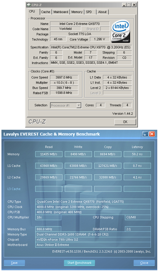
Our Intel QX9770 at 400MHz FSB with the memory running "linked 'n synced" at DDR3-1600 performs beautifully, pulling down well over 11GB/s in memory read performance.
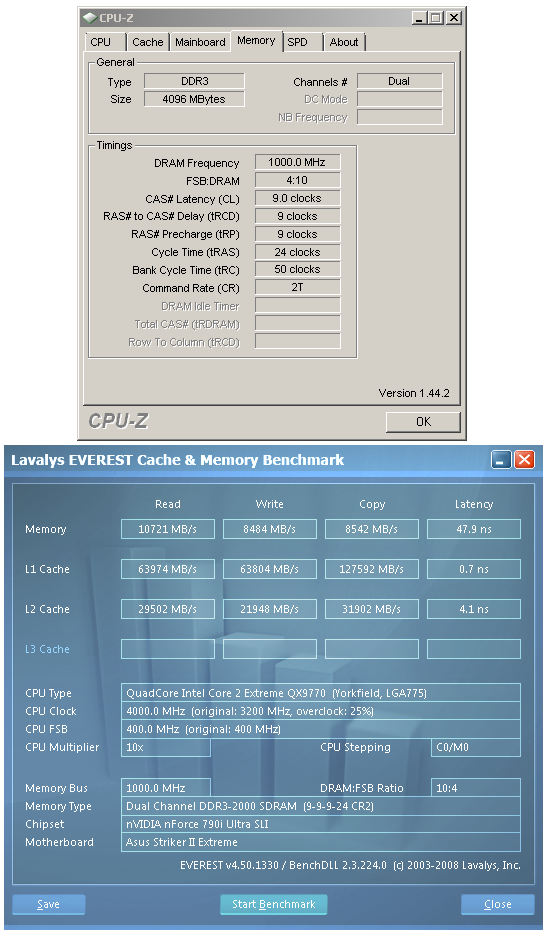
Our attempt at gaining more performance backfires when we unlink the memory and go to DDR3-2000. We actually lose more than 500MB/s in memory read performance at a higher memory speed.
The first option, Auto, represents whatever ratio is needed to set the memory for DDR3-1333 operation if a 333MHz (1333MT/s) CPU or 400MHz (1600MT/s) CPU is installed or DDR3-1066 operation if a 266MHz (1066MT/s) CPU is installed. This means Sync Mode (2:1) is set for every installed CPU with the exception of the QX9770, which actually defaults to a 6:5 ratio. In this particular case, a loss of performance will ensue unless the user (mandating DDR3-1600 operation) sets Sync Mode, and not Auto. Do yourself a favor and buy memory rated no lower than DDR3-1600 if you plan on ever moving up to the QX9700 or overclocking your CPU with this board to 400MHz FSB and higher. Do not let the relatively low prices of "value" DDR3 rated at 1333 or lower tempt you into a purchase unless you know it will overclock well.
FSB (QDR), MHz This is the target FSB, displayed in quad-data rate (QDR) format. Just realize that you should quadruple (x4) the actual base frequency desired when entering this value. The actual FSB (actual FSB MHz - quad-pumped) is shown directly below this setting and should always match what you enter here.
MEM (DDR), MHz This option that allows the user to type in a target memory speed and will only be available for direct edit when choosing "Unlinked" under FSB - Memory Clock Mode. Otherwise, this is automatically filled in based on the current FSB (QDR), MHz and FSB - Memory Ratio.
You may notice a slight offset from this target frequency, reflected in Actual MEM (DDR), MHz, when clocking your memory using the "Unlinked" mode of operation. This is normal and is due to the limited number of actual non-standard dividers implemented by the chipset used to give the illusion of fully dissociated clocking domains for the system and memory busses.
LDT Frequency - [1x ~ 5x] LDT (Lightning Data Transport) technology, licensed by NVIDIA from AMD, provides the interface pathway used to connected the 790i SPP with the 570 MCP. This setting should really be named "LDT Multiplier" as the final SPP-to-MCP link speed is set by multiplying this value by SPP<->MCP Ref Clock, MHz.
PCIE Bus, Slot 1 & 2 MHz PCIe x16 Slots 1 and 2 (blue in color) are PCI Express 2.0 compatible slots and should be used for the primary graphics controllers when running SLI. This field controls the base link speed between devices installed in these slots and the 790i SPP. Changing this from the default 100MHz value would always hang our Vista x64 system during OS load when the video drivers were first initialized.
PCIE Bus, Slot 3, MHz PCIe x16 Slot 3 (white in color) is the single PCI Express 1.x compatible slot. This field controls the base link speed between the device installed in this slot and the 570 MCP. Overclocking this interface will have absolutely no effect on graphics performance unless a third graphics controller is installed in this slot and is being used for 3-way SLI.
SPP<->MCP Ref Clock, MHz This field sets the base frequency of the SPP-to-MCP LDT interface link. In theory, a higher link speed, coupled with the highest possible multiplier (LDT Frequency) - resulting in the maximum stable link speed - should result in better system performance. However, unless you are running a 3-way SLI configuration and can show real gains by overclocking this interface, this is best left set to Auto. Unusually high link speeds have the potential to cause problems such as disk corruption, loss of RAID arrays, or memory access errors for DMA-connected devices.
SLI-Ready Memory - [Disabled, CPUOC 0% ~ CPUOC 5%, CPUOC MAX] Leave this setting on Disabled when manually overclocking memory. Selecting any other option will set DDR3-2000 memory operation - we were unable to measure any difference between any of the "CPU OC x%" options. Make sure you either manually adjust your memory timings or leave them on "Auto" if you plan on overclocking your memory this way.
Complete BIOS Tuning Guide - "Memory Timing Setting"
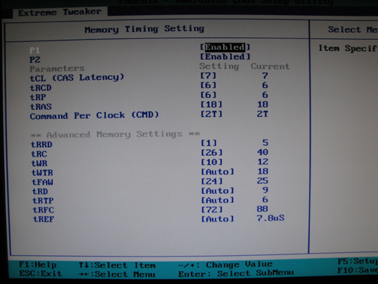
Memory Timing Setting
P1 - [Auto, Enabled] We can tell you this setting optimizes internal MCH latencies when setting an FSB of 475MHz or greater, but the exact functionality is unknown at this time. Enable this option when overclocking above 475FSB to gain back some memory read performance and improve memory access latencies. Below 475FSB, this option has no effect (Auto maps to Enabled by default). You may need to increase NB Core Voltage (SPP Voltage) when this setting is Enabled.
P2 - [Auto, Enabled] This setting should also be Enabled if possible when clocking above 475FSB. Typically, you will have problems with "P2" if your system in unstable with "P1" Enabled. Enabling both "P1" and "P2" will result in the greatest memory read performance improvement.
tCL (CAS Latency) - [Auto, 5 ~ 18] As a rule of thumb, use 6 below DDR3-1600, 7 from DDR3-1600 to about DDR3-1830, 8 from DDR3-1830 to about DDR-2000 and 9 for anything above DDR3-2000. Not all memory is the same so you will need to experiment to see what works best. Besides the actual memory speed, the selection of this value has one of the greatest impacts on the memory voltage required for stable operation (lower values leads to higher voltages).
tRCD (RAS to CAS Delay) - [Auto, 1 ~ 15] You cannot go wrong setting this to the same value as tCL. Sometimes you can set this to tCL -1 without the need for any additional voltage; just do not expect a big change in memory read bandwidth.
tRP (Row Precharge) - [Auto, 1 ~ 15] Like tRCD, set this to the same value as tCL or use tCL -1. Typically, if memory will handle a tRCD of tCL -1 then you may be able to get away with tRCD -1 one for tRP. Again, try different values and go with the lowest number you can get away with without the need for excessive memory voltage.
tRAS (Active to Precharge Delay) - [Auto, 1 ~ 63] Never set a tRAS lower than tRCD + tCL + 2. Contrary to popular belief, tRAS is not as much an actual timing as it is a minimum cycle time. Lower values are almost guaranteed not to improve memory performance but stability can go south in a hurry if you are too aggressive with this timing.
Command Per Clock - [Auto, 1 clock, 2 clock] Generally speaking, 1T command timing should be good up to about DDR3-1860 with 2GB of memory. Save yourself the hassle and use 2T whenever overclocking with 4GB or 8GB of DDR3.
tRRD (RAS to RAS Delay) - [Auto, 1 ~ 15] We recommend you set this value to 1 and leave it there.
tRC (Bank Cycle Time) - [Auto, 1 ~ 63] This is arguably one of the most important timings when it comes to memory performance with NVIDIA chipsets. The rule when it comes to tRC is you should set it no lower than tCL + tRAS + 2. Even small reductions in this timing can bring about large decreases in memory access latencies.
tWR (Write Recovery Time) - [Auto, 5, 6, 7, 8, 10, 12] Tighten this to 10 if you can. Some memory will go as low as 8 if you feed it enough voltage.
tWTR (Write to Read Delay) - [Auto, 1 ~ 31] This setting is best left on Auto.
tFAW (Four Active Window Delay) - [Auto, 1 ~ 63] Try setting this to whatever you use for tRC. Those that are overclocking 8GB of DDR3 may need to loosen this significantly above DDR3-1600 or so.
tRD (Read Delay) - [Auto, 1 ~ 15] This timings was added at our bequest starting with BIOS 0504. Unfortunately, the chipset does not respond to this option in the manner in which an Intel chipset would. For now, ignore this timing as if it did not exist (leave on Auto).
tRTP (Read to Precharge Delay) - [Auto, 1 ~ 15] This setting is best left on Auto.
tRFC (Row Refresh Cycle Time) - [Auto (0), Manual to 255] Set a tRFC of at least 72 when clocking 8GB of DDR3 above DDR3-1600. Otherwise, the board handles adjusting this option automatically quite well. A small amount of memory read performance can sometimes be gained with moderately lower values. Go too far though and you will be greeted with a BSOD during OS load.
tREF (Refresh Period) - [Auto, 3.9, 7.8] Leave this on Auto as the correct value is read from your modules SPD (typically 7.8μS).
Complete BIOS Tuning Guide - "Over Voltage"
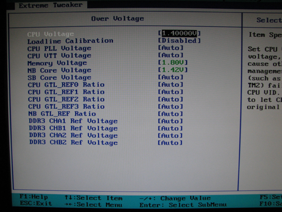
Over Voltage
CPU Voltage - [Auto, 1.10000 ~ 2.40000 in 0.00625 steps] This setting controls the processor supply voltage by manually adjusting the target CPU VID.
Our measurements have shown the ASUS Striker II Extreme to have a nominal load line impedance (RLL) of approximately 0.80mΩ meaning that for each ampere (A) drawn by the processor the regulated supply voltage will droop 0.8mV. Given this, a 45nm quad-core QX9650 CPU with a full-load power consumption of 80W should draw about 65A, resulting in a total drop of around 0.05V from idle to full-load.
Loadline Calibration - [Enabled, Disabled] Setting Enabled will effectively remove any negative feedback in the CPU supply voltage regulation circuit. This means that there will be little to no difference between the CPU supply voltage at idle and full-load. This does not mean however that there will be no offset seen between the idle voltage and the CPU Voltage VID as selected in BIOS. Disabled follows the Intel specification and allows the CPU supply voltage to droop under load as properly designed. We recommend you leave this Disabled and increase CPU Voltage as needed to satisfy the minimum operating voltage needed under load.
CPU PLL Voltage - [Auto, 1.50 ~ 3.00 in 0.02 steps] Selecting a higher PLL (phase lock-loop) voltage may help the installed CPU clock higher or may assist with maintaining stability when operating at higher FSB speeds. Most users will find they do not need to set this to anything above 1.50. Exercise caution when experimenting with higher values as there have been reported cases of CPUs losing cores after being subjected to voltages in excess of about 2.00V.
CPU VTT Voltage - [Auto, 1.20 ~ 2.46 in 0.02 steps] VTT is the termination voltage for data lines used to interface the MCH with the CPU die(s) via the Front Side Bus. Higher values can provide additional FSB overclocking margin, especially with 45nm dual-core processors and quad-cores CPUs in general. We have never found any additional gains to be had above 1.36 when using air- or water-cooling. Setting Auto should default to 1.10V for 45nm CPUs and 1.20V for 65nm CPUs. Knowing this, there appears to be a dead band between 1.10V and 1.20V where intermediate values cannot be selected - we are working with ASUS engineering to get this corrected.
Memory Voltage - [Auto, 1.50 ~ 3.10 in 0.02 steps] DDR3 memory is rated for standard operation at just 1.5V with most performance memory kits specifying the use of voltages between 1.75V and 1.95V inclusive. Increasing the memory voltage will have a direct impact on the ability to run the installed memory at higher frequencies, with tighter timings, or both. This voltage will droop slightly under load, so consider this when selecting the appropriate value. Our recommendation is never to exceed the manufacturer's maximum warranted voltage. With that said, values in excess of about 2.30V with DDR3 are a death sentence.
NB Core Voltage - [Auto, 1.30 ~ 2.20 in 0.02 steps] This is the main power supply voltage for the 790i SPP. Any of the following adjustments may require an increase in this voltage: higher memory operating frequency, tighter memory timings, enabling P1 and/or P2, the use of additional memory modules (including higher-density modules), and increases in PCIe Slot 1/Slot 2 base link speeds. We were able to reach DDR3-2000 speeds (500FSB) using 4x2GB of OCZ DDR3 with only 1.52. This is near full load for this chipset, suggesting that higher voltages will only lead to additional heating and eventual instabilities.
SB Core Voltage - [Auto, 1.50 ~ 1.85 in 0.05 steps] This is the main power supply voltage for the 570 MCP. Leave this voltage set to 1.50 unless you increase PCIE Bus, Slot 3, MHz, LDT Frequency, and/or SPP<->MCP Ref Clock, MHz and find instabilities due to the change(s).
Complete BIOS Tuning Guide - "Over Voltage" (Cont'd)
CPU GTL_REF(0~4) Ratio - [Auto, Default, -226mV ~ +224mV] Gunning Transceiver Logic (GTL) voltages are nothing more than reference thresholds used by the CPU and SPP (MCH) in determining if the voltage potential on a FSB data or address signal line is intended to represent either a logic level 1 (high) or logical level 0 (low). These voltages are generated by the motherboard, usually though the use of precision voltage dividers or high-accuracy, programmable digital potentiometers. Although the most common way to specify these values is as a percentage (or ratio) of full scale CPU VTT Voltage, NVIDIA has decided to provide these settings as simple offsets meaning a little math will be involved if you want to make a change.
These reference values are particularly important when overclocking quad-core CPUs, especially when venturing above about 475MHz FSB. The ability to tune these values per die can mean the difference between achieving a stable overclock at 475FSB and one at 500FSB. The real power seen in GTL reference tuning comes in the ability to provide each quad-core die with separate reference values. (Recall that current quad-cores from Intel are an MCM design consisting of two dual-core dies on a single substrate package.)
This can get tricky though as each die receives two GTL reference voltages - one for the FSB Data Bus (running at the full FSB transfer rate) and one for the FSB Address Bus (running at half the FSB transfer rate). This means CPU GTL_REF0 Ratio is for the Core 0/1 Data Bus, CPU GTL_REF1 Ratio is for the Core 2/3 Data Bus, CPU GTL_REF2 Ratio is for the Core 0/1 Address Bus, and CPU GTL_REF3 Ratio is for the Core2/3 Address Bus. CPU GTL_REF2 Ratio and CPU GTL_REF3 Ratio will have no affect with a dual-core CPU installed, in which case CPU GTL_REF0 Ratio is for the Core 0/1 Data Bus and CPU GTL_REF1 Ratio is for the Core 0/1 Address Bus. As a rule, adjustments are normally made to FSB Data Bus values first. These lines are consistently heavily loaded and as such are more susceptible to the detrimental effects of reduced signaling margins.
Intel's GTL specification dictates that each reference voltage should be tightly controlled as 67% of the current VTT voltage (0.67 times CPU VTT Voltage). Typically, changes in VTT are automatically compensated with standard voltage divider circuits dedicated to the generation of each GTL reference voltage. Historical data has shown that dual-core CPUs (in particular 45nm dual-cores) often clock to higher FSB levels when the GTL reference values are closer to 63 ~ 64% of VTT while quad-core CPUs usually need the full strength value or even a little more voltage (67 ~ 70% of VTT).
As an exercise in the application of basic math, consider the following. With VTT at 1.10V, the GTL reference voltages at 67% would be 0.737V (0.67 times 1.10V). If VTT increased to 1.26V, the new GTL reference voltage would be 0.844V, calculated the same as before. If we wanted to adjust this down to 63%, we would simply multiply the current VTT voltage by the difference between the actual and desired percentages of full scale VTT (67% minus 63% equals 4% or 0.04) and then convert this to mV by multiplying by 1000. At 1.26V, the result would be 50mV and since we want to reduce the GTL reference voltage we would pick the value closest to -50mV. Sometimes tweaking VTT slightly up or down can help if none of the available values is close enough the desired offset. Of course, you will need to repeat the calculation using the new VTT.
Proper GTL reference level tuning can sometimes allow for a dramatic reduction in VTT and in some severe cases even permits the use of a lower core supply voltage (Vcore). The most recent x64 build of Prime95, version 25.6 build 6, provides an excellent means for testing the effectiveness of CPU-specific GTL tuning. Simply load the program, select the Blend type Torture Test, and watch for any instance to drop out. Note the instance number (which will correlate to the core in question), reset and enter the BIOS, make a small adjustment to the corresponding GTL reference value(s), and then start a new test run. If the test runs for a longer period of time then you can be confident that you are at least moving in the right direction. Continue this process until the system is sufficiently stable with the current settings.
Those that want to know more about GTL reference voltages and related tuning issues are encouraged to carefully examine more in-depth articles on the subject posted here and here.
NB GTL_REF Ratio - [Auto, Default, -126mV ~ +160mV] The NB (SPP) GTL reference voltage provides the same functionality as those for the CPU, the only difference being that the Northbridge uses only a single value. Tuning in the right GTL reference voltage (usually near the nominal 67% value) can sometimes lead to lower stable VDIMM requirements.
DDR3 CHA(1~2)/CHB(1~2) Ref Voltage - [Auto, Default, -126mV ~ +160mV] These voltages work like GTL references for memory, except that VTT for the memory is defined as one-half VDIMM. Small adjustments in either direction can sometimes bring additional stability or higher memory overclocks; however, testing the effectiveness of any change is exceedingly difficult and time consuming. Most of the time these are better off simply left on Auto.
Complete BIOS Tuning Guide - "CPU Configuration"
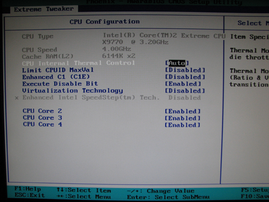
CPU Configuration
CPU Internal Thermal Control - [Auto, Disabled] Always leave this on Auto as disabling internal thermal control can have unknown affects on system operation. According to sources at Intel, thermal control is required to be active if the CPU is expected to correctly function within specifications.
Limit CPUID MaxVal - [Enabled, Disabled] Some legacy operating systems (i.e. Windows NT SP2 and older) are unable to properly deal with the CPUID x86 opcode when called using operands greater than 3. The problem is that the boot code for these older system was written to query the CPU for the highest supported value and then to call a routine using this value. Unfortunately, the programmers did not have the foresight to account for future processors with higher values and the OS crashes with a BSOD due to the unhandled exception in a routine running with kernel mode privileges.
The result is a general incompatibility between these newer CPUs (with a maximum supported CPUID value of 4) and these older operating systems. Set this to Enabled if you experience just such a problem, otherwise leave this Disabled. Beware that improperly enabling this setting with Windows 2000, XP, or any flavor of Vista can cause serious performance problems.
Enhanced C1 (C1E) - [Enabled, Disabled] C1E functions to reduce the CPU multiplier to 6.0x when idling or running in load-load conditions. This can sometimes provide a small degree of power savings, especially if the system is highly overclocked to begin with. Most users find the constant switching between the idle and load frequencies annoying, besides which a small performance penalty is experienced during each transition. We usually disable this setting and recommend you do the same if you are building your system for gaming purposes.
Execute Disable Bit - [Enabled, Disabled] The Execute Disable (NX) Bit is typically used as a form of hardware protection against the execution of malicious code. This bit is part of the page table descriptor used to mark the memory page table as executable or not. This way programs that purposefully cause buffer overflows that end up spilling into the memory address space of other processes cannot execute injected data unless the page is specifically marked as containing executable code. Enabling this feature will force Physical Address Extension (PAE) Mode when running a 32-bit Windows OS regardless of the amount of system memory installed. This is because the NX bit resides at bit 63 of the page table entry and page table entries are only 32 bits in length with PAE disabled. 64-bit operating systems always run in PAE Mode. Enabling this feature has never negatively affected our ability to overclock.
Virtualization Technology - [Enabled, Disabled] This setting controls whether or not the BIOS masks requests sent to the CPU in determining whether or not Virtualization Technology (VT) is supported. Disabling this setting ensures the system cannot run any code pertaining to system virtualization. We usually leave this Disabled unless we have a good reason to enable it.
Enhanced Intel SpeedStep(tm) Tech. - [Enabled, Disabled] Although some BIOS releases may allows this features to be alternately Disabled or Enabled, it has no affect unless the installed CPU is capable of conducting power state transitions and no desktop chipset contains this feature set (yet). This option should be grayed out unless you have some special CPU have not encountered.
CPU Core 2/3/4 - [Enabled, Disabled] This setting merely controls a mask used by the BIOS in determining which cores are advertised as available for use by the host systems. Disabling cores can sometimes allow a quad-core CPU to function more like a dual-core CPU when it comes to FSB clocking. Numbering the cores from 1 is a mistake in our opinion; this option should really read "CPU Core 1/2/3".
Complete BIOS Tuning Guide - "Spread Spectrum Control"
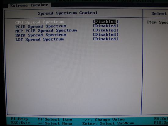
Spread Spectrum Control
Spread spectrum controls are really added to motherboards for one purpose only - they are sometimes needed so that a device for sale within the US can include a legitimate Declaration of Conformity stating compliance with Part 15 of the Federal Communications Commission (FCC) Rules. This stipulates that operation of the device (motherboard), (a) may not cause harmful interference, and (b) must accept any interference received, including interference that may cause undesired operation. Sales of electronic devices within the US require the strict observation of all FCC rules and regulations.
As a general requirement, every motherboard must be capable of generating and distributing more than one common clocking signal used to coordinate latching times as needed for the transfer and receipt of data across the many high-speed interfaces found in today's systems. Because it is uncommon for different busses to share similar operating frequencies, and because each must be kept independent of the others, a significant portion of motherboard resources are spent locating, monitoring, and regulating these circuits. Each circuit must include a reference frequency, or known base frequency, from which all other frequencies can be derived. A local oscillator usual provides this functionality.
The problem is these oscillators can sometimes cause electromagnetic interference (EMI) centered about their operating frequencies. In an effort to prevent these types of undesired interferences the FCC, an independent licensing organization for devices capable of transmitting electromagnetic signals, either intended or otherwise, operating under the purview of the US government, enacted "Rule 15," effectively limiting the output power of such devices.
Engineers, looking for a way to meet regulation, began using a method for limiting such interferences called spread spectrum clocking. Spread spectrum clocking causes the signal regulation circuit to slightly vary the frequency about the target frequency, effectively "spreading" the power over a somewhat larger frequency band. The method of operation can be used to control system output power below the FCC standard limits, allowing for a claim of full compliance.
As you can imagine, even the smallest variation in a clocking signal can be enough to create data transfer errors. The fundamentals of overclocking demand the cleanest, purest signal possible, which is why spread spectrum should always be disabled unless you have a good reason to enable it. Ergo, CPU Spread Spectrum, PCIE Spread Spectrum, MCP PCIE Spread Spectrum, SATA Spread Spectrum, and LDT Spread Spectrum should all be set to Disabled.
Final Thoughts and Recommendations
NVIDIA's 790i has already proven itself
a very capable platform for overclocking, something we did not expect to say considering
this is the first (and last?) DDR3 memory controller from the green team. Performance
is great, overclocking is easy, and NVIDIA has even managed to keep power consumption
in check. By every account, the 790i is a real contender when placed side-by-side
with Intel's X48 Express chipset. However, there is a dark side to this chipset. We are working with NVIDIA at this time to figure out our random data corruption problems. We have lost several drive images during testing. While we expect to corrupt drive images when pushing a system beyond its boundaries, this problem has occurred numerous times with fairly ordinary overclocks. Typically, settings around 400FSB (QDR 1600) and memory set at DDR3-1600 with relaxed timings around 7-7-7-18 resulted in random, but not repeatable corrupted images in Vista. NVIDIA is busily testing at this point and we will have an update shortly.
As we see it, the extra $100 premium beyond the cost of even the most obnoxiously priced Intel-based motherboard buys you the right to run your NVIDIA GPUs in SLI, assuming you can afford more than one after shelling out for the ASUS Striker II Extreme. Of course, once you have your hands on this board you might find you will stop at nothing to get SLI up and running. NVIDIA's second shot at Quad-SLI with a pair of GeForce 9800 GX2 cards could be very tempting if driver performance ever catches up with the hype. There is something special about running Crysis with "Very High Settings" in DX10 at 1920x1200.
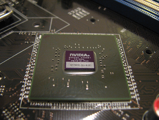
I think this NVIDIA 790i Ultra SPP just winked at me.
DDR3 prices have also made the idea of moving to either X48 or 790i a whole lot less painful than it would have been just a few short months ago. Great clocking and relatively inexpensive 2GB kits of DDR3 are starting to show up at all our favorite online retailers. We were able to find 2GB kits like the Patriot Viper rated at DDR3-1600 with 7-7-7 timings for under $200 without too much trouble. To date, all of our experiences with DDR3 memory have shown the DDR3-1600 kits to be incredible performers when it comes to overclocking.
If you're still buying DDR2 and you're serious about overclocking, you're buying yesterday's technology. That might be fine for the price-conscious enthusiasts, but if you're considering the purchase of a $300+ motherboard and $1000 CPU we have to strongly recommend making the move to DDR3. It's also worth noting that once Intel's Nehalem architecture hits the market - which should occur later this year - you can kiss DDR2 compatibility on the latest Intel platforms goodbye. At that point, you'll need to purchase DDR3 memory if you want to keep up with the Joneses - though what sort of prices and performance we'll see for DDR3 by the time this occurs is anyone's guess. Our advice for enthusiasts is to send your DDR2 packing and never look back when it comes time to purchase a new high-end motherboard.
Frankly, some of us find all this talk about overly expensive products depressing. What happened to expecting to pay top dollar for premium components? True, there are those out there that are able to buy mainstream products and push them well beyond their rated capabilities for next to nothing. Shoot, that is the very definition of overclocking right there. However, when did we become entitled to low prices when it comes to picking up motherboards claiming to be ultimate overclockers? It is one thing to pay a lot and get a little, but when a product delivers everything it promises and more, complaining does not make sense. We will tell you straight up, the ASUS Striker II Extreme is a serious piece of hardware, and if you want to play with the big boys, you had better be prepared to throw the cash down!


