Original Link: https://www.anandtech.com/show/15862/intel-launches-cooper-lake-3rd-generation-xeon-scalable-for-4p8p-servers
Intel Launches Cooper Lake: 3rd Generation Xeon Scalable for 4P/8P Servers
by Dr. Ian Cutress on June 18, 2020 9:00 AM EST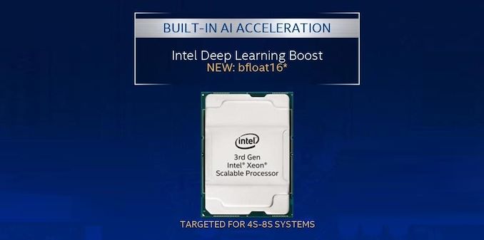
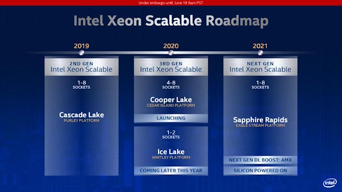
We’ve known about Intel’s Cooper Lake platform for a number of quarters. What was initially planned, as far as we understand, as a custom silicon variant of Cascade Lake for its high-profile customers, it was subsequently productized and aimed to be inserted into a delay in Intel’s roadmap caused by the development of 10nm for Xeon. Set to be a full range update to the product stack, in the last quarter, Intel declared that its Cooper Lake platform would end up solely in the hands of its priority customers, only as a quad-socket or higher platform. Today, Intel launches Cooper Lake, and confirms that Ice Lake is set to come out later this year, aimed at the 1P/2P markets.
Count Your Coopers: BFloat16 Support
Cooper Lake Xeon Scalable is officially designated as Intel’s 3rd Generation of Xeon Scalable for high-socket count servers. Ice Lake Xeon Scalable, when it launches later this year, will also be called 3rd Generation of Xeon Scalable, except for low core count servers.
For Cooper Lake, Intel has made three key additions to the platform. First is the addition of AVX512-based BF16 instructions, allowing users to take advantage of the BF16 number format. A number of key AI workloads, typically done in FP32 or FP16, can now be performed in BF16 to get almost the same throughput as FP16 for almost the same range of FP32. Facebook made a big deal about BF16 in its presentation last year at Hot Chips, where it forms a critical part of its Zion platform. At the time the presentation was made, there was no CPU on the market that supported BF16, which led to this amusing exchange at the conference:
BF16 (bfloat16) is a way of encoding a number in binary that attempts to take advantage of the range of a 32-bit number, but in a 16-bit format such that double the compute can be packed into the same number of bits. The simple table looks a bit like this:
| Data Type Representations | ||||||
| Type | Bits | Exponent | Fraction | Precision | Range | Speed |
| float32 | 32 | 8 | 23 | High | High | Slow |
| float16 | 16 | 5 | 10 | Low | Low | 2x Fast |
| bfloat16 | 16 | 8 | 7 | Lower | High | 2x Fast |
By using BF16 numbers rather than FP32 numbers, it would also mean that memory bandwidth requirements as well as system-to-system network requirements could be halved. On the scale of a Facebook, or an Amazon, or a Tencent, this would appeal to them. At the time of the presentation at Hot Chips last year, Facebook confirmed that it already had silicon working on its datasets.
Doubling Socket-to-Socket Interconnect Bandwidth
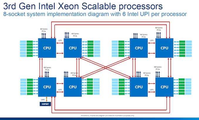
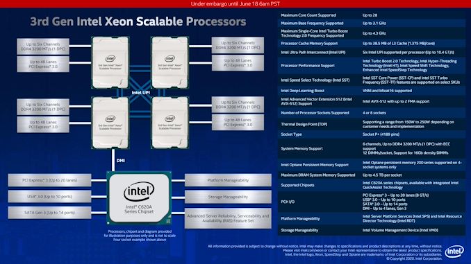
The second upgrade that Intel has made to Cooper Lake over Cascade Lake is in socket-to-socket interconnect. Traditionally Intel’s Xeon processors have relied on a form of QPI/UPI (Ultra Path Interconnect) in order to connect multiple CPUs together to act as one system. In Cascade Lake Xeon Scalable, the top end processors each had three UPI links running at 10.4 GT/s. For Cooper Lake, we have six UPI links also running at 10.4 GT/s, however these links still only have three controllers behind them such that each CPU can only connect to three other CPUs, but the bandwidth can be doubled.
This means that in Cooper Lake, each CPU-to-CPU connection involves two UPI links, each running at 10.4 GT/s, for a total of 20.8 GT/s. Because the number of links is doubled, rather than an evolution of the standard, there are no power efficiency improvements beyond anything Intel has done to the manufacturing process. Note that double the bandwidth between sockets is still a good thing, even if latency and power per bit is still the same.
Intel still uses the double pinwheel topology for its eight socket designs, ensuring at max two hops to any required processor in the set. Eight socket is the limit with a glueless network – we have already seen companies like Microsoft build servers with 32 sockets using additional glue logic.
Memory and 2nd Gen Optane
The third upgrade for Cooper Lake is the memory support. Intel is now supporting DDR4-3200 with the Cooper Xeon Platinum parts, however only in a 1 DIMM per channel (1 DPC) scenario. 2 DPC is supported, but only at DDR4-2933. Support for DDR4-3200 technically gives the system a boost from 23.46 GB/s per channel to 25.60 GB/s, an increase of 9.1%.
The base models of Cooper Lake will also be updated to support 1.125 TiB of memory, up from 1 TB. This allows for a 12 DIMM scenario where six modules are 64 GB and six modules are 128 GB. One of the complaints about Cascade Xeons was that in 1 TB mode, it would not allow for an even capacity per memory channel when it was filled with memory, so Intel have rectified this situation. In this scenario, it means that the six 128 GB modules could also be Optane. Why Intel didn’t go for the full 12 * 128 GB scenario, we’ll never know.
The higher memory capacity processors will support 4.5 TB of memory, and be listed as ‘HL’ processors.
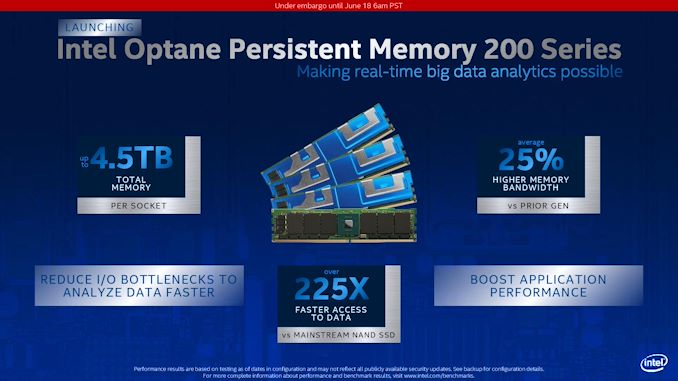
Cooper Lake will also support Intel’s second generation 200-series Optane DC Persistent Memory, codenamed Barlow Pass. 200-series Optane DCPMM will still available in 128 GB, 256 GB, and 512 GB modules, same as the first generation, and will also run at the same DDR4-2666 memory speed. Intel claims that this new generation of Optane offers 25% higher memory bandwidth than the previous generation, which we assume comes down to a new generation of Optane controller on the memory and software optimization at the system level.
Intel states that the 25% performance increase is when they compare 1st gen Optane DCPMM to 2nd gen Optane DCPMM at 15 W, both operating at DDR4-2666. Note that the first-gen could operate in different power modes, from 12 W up to 18 W. We asked Intel if the second generation was the same, and they stated that 15 W is the maximum power mode offered in the new generation.
Socket, Silicon, and SKUs
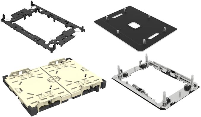
Cooper Lake Xeon Scalable ushers in a new socket, given that it is difficult to add in UPI links without adding additional pins. The new socket is known as LGA4189, for which there will be two variants: LGA4189-4 and LGA4189-5. When asked, Intel stated that Cooper Lake supports the LGA4189-5 socket, however when we asked an OEM about the difference between the sockets, we were told it comes down to the PCIe version.
LGA4189-5, for Cooper Lake, uses PCIe 3.0. LGA4189-4, which is for Ice Lake we were told, will be PCIe 4.0 Nonetheless, Intel obfuscates the difference by calling both of them ‘Socket P+’. It’s not clear if they will be interchangeable, given that technically PCIe 4.0 can work in PCIe 3.0 mode, and a PCIe 3.0 chip can work in a PCIe 4.0 board at PCIe 3.0 speeds, but it will come down to how the UPI links are distributed, and any other differences.
We've since been told that the design of the socket is meant to make sure that Ice Lake Xeon processors should not be placed in Cooper Lake systems, however Cooper Lake processors will be enabled in systems built for Ice Lake.
We’re unsure if that means that LGA4189 / Socket P+ will be a single generation socket or not. Sapphire Rapids, mean to be the next generation Xeon Scalable, is also set for 2nd gen Optane support, which could imply a DDR4 arrangement. If Sapphire Rapids supports CXL, then that’s a PCIe 5.0 technology. There’s going to be a flurry of change within Intel’s Xeon ecosystem it seems.
On the silicon side, Intel has decided to not disclose the die configurations for Cooper Lake. In previous generations of Xeon and Xeon Scalable, Intel would happily publish that it used three different die sizes at the silicon level to separate up the core count distribution. For Cooper Lake however, we were told that ‘we are not disclosing this information’.
I quipped that this is a new level of secrecy from Intel.
Given that Cooper Lake will be offered in variants from 16 to 28 cores, and is built on Intel’s 14nm class process (14+++?), we can at least conclude there is a ’28 core XCC’ variant. Usually on these things the L3 cache counts are a good indicator of something smaller is going to be part of the manufacturing regime, however each processor sticks to the 1.375 MB of L3 cache per core configuration.
This leads us onto the actual processors being launched. Intel is only launching Platinum 8300, Gold 6300, and Gold 5300 versions of Cooper Lake, given that its distribution is limited to four socket systems or greater, and to high scale OEMs only. TDPs start at 150-165 W for the 16-24 core parts, moving up to 205-250 W for the 18-28 core parts. The power increases come from a combination of slight frequency bumps, higher memory speed support, and double the UPI links.
| Intel 3rd Gen Xeon Scalable Cooper Lake 4P/8P |
||||||||||
| AnandTech | Cores | Base Freq |
1T Turbo |
DDR4 1DPC |
DDR4 2DPC |
DDR4 TiB |
TDP W |
4P 8P |
Intel SST |
Price |
| Xeon Platinum 8300 | ||||||||||
| 8380HL | 28C | 2900 | 4300 | 3200 | 2933 | 4.5 | 250 | 8P | No | $13012 |
| 8380H | 28C | 2900 | 4300 | 3200 | 2933 | 1.125 | 250 | 8P | No | $10009 |
| 8376HL | 28C | 2600 | 4300 | 3200 | 2933 | 4.5 | 205 | 8P | No | $11722 |
| 8376H | 28C | 2600 | 4300 | 3200 | 2933 | 1.12 | 205 | 8P | No | $8719 |
| 8354H | 18C | 3100 | 4300 | 3200 | 2933 | 1.12 | 205 | 8P | No | $3500 |
| 8353H | 18C | 2500 | 3800 | 3200 | 2933 | 1.12 | 150 | 8P | No | $3003 |
| Xeon Gold 6300 | ||||||||||
| 6348H | 24C | 2300 | 4200 | - | 2933 | 1.12 | 165 | 4P | No | $2700 |
| 6328HL | 16C | 2800 | 4300 | - | 2933 | 4.5 | 165 | 4P | Yes | $4779 |
| 6328H | 16C | 2800 | 4300 | - | 2933 | 1.12 | 165 | 4P | Yes | $1776 |
| Xeon Gold 5300 | ||||||||||
| 5320H | 20C | 2400 | 4200 | - | 2933 | 1.12 | 150 | 4P | Yes | $1555 |
| 5318H | 18C | 2500 | 3800 | - | 2933 | 1.12 | 150 | 4P | No | $1273 |
| All CPUs have Hyperthreading | ||||||||||
Quite honestly, Intel's naming scheme is getting more difficult to follow. Every generation of Xeon Scalable becomes a tangled mess of feature separation.
No prices are attached to any of the Cooper Lake processors from our briefings, but Intel did publish them in its price document. We can compare the top SKUs from the previous generations, as well as against AMD's best.
| Intel Xeon 8x80 Compare | ||||
| Xeon 8180M |
Xeon 8280L |
Xeon 8380HL |
AnandTech | EPYC 7H12 |
| Skylake | Cascade | Cooper | Platform | Rome |
| 14nm | 14+ nm | 14++ nm? | Node | 7nm + 14nm |
| $13011 | $13012 | $13012 | Price | ~$8500 |
| 28 C | 28 C | 28 C | Cores | 64 C |
| 2500 MHz | 2700 MHz | 2900 MHz | Base | 2600 MHz |
| 3800 MHz | 4000 MHz | 4300 MHz | 1T Turbo | 3300 MHz |
| 6 x 2666 | 6 x 2933 | 6 x 3200 | DDR4 | 8 x 3200 |
| 1.5 TiB DDR4 | 4.5 TiB Optane | 4.5 TiB Optane | Max Mem | 4 TiB DDR4 |
| 205 W | 205 W | 250 W | TDP | 280 W |
| 1P to 8P | 1P to 8P | 1P to 8P | Sockets | 1P, 2P |
| 3 x 10.4 GT/s | 3 x 10.4 GT/s | 6 x 10.4 GT/s | UPI/IF | 64 x PCIe 4.0 |
| 3.0 x48 | 3.0 x48 | 3.0 x48 | PCIe | 4.0 x128 |
| AVX-512 F/CD/BW/DQ |
AVX-512 F/CD/BW/DQ + VNNI |
AVX-512 F/CD/BW/DQ + VNNI +BF16 |
AVX | AVX2 |
The new processor improves on base frequency by +200 MHz and turbo frequency by +300 MHz, but it does have that extra 45 W TDP.
Compared to AMD’s Rome processors, the most obvious advantages to Intel are in frequency socket support, the range of vector extensions supported, and also memory capacity if we bundle in Optane. AMD’s wins are in has core counts, price, interconnect, PCIe count, and memory bandwidth. However, the design of Intel’s Cooper Lake with BF16 support is ultimately for customers who weren’t looking at AMD for those workloads.
We should also point out that these SKUs are the only ones Intel is making public. As explained in previous presentations, more than 50% of Intel's Xeon sales are actually custom versions of these, with different frequency / L3 cache / TDP variations that the big customers are prepared to pay for. In Intel's briefing, some of the performance numbers given by its customers are based on that silicon, e.g. 'Alibaba Customized SKU'. We never tend to hear about these, unfortunately.
Platform
As hinted above, Intel is still supporting PCIe 3.0 with Cooper Lake, with 48 lanes per CPU. The topology will also reuse Intel’s C620 series chipsets, providing 20 more lanes of PCIe 3.0 as well as USB 3.0 and SATA.
Intel did not go into items such as VROC support or improvements for this generation, so we expect support for those to be similar to Cascade Lake.
Performance and Deployments
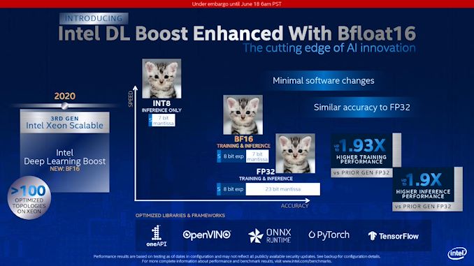
As part of the discussion points, Intel stated that it has integrated its BF16 support into its usual array of supported frameworks and utilities that it normally defines as ‘Intel DL Boost’. This includes PyTorch, TensorFlow, OneAPI, OpenVino, and ONNX. We had a discussion with Wei Li, who heads up Intel’s AI Software Group at Intel, who confirmed to us that all these libraries have already been updated for use with BF16. For the high level programmers, these libraries will accept FP32 data and do the data conversion automatically to BF16, however the functions will still require an indication to use BF16 over INT8 or something similar.
When speaking with Wei Li, he confirmed that all the major CSPs who have taken delivery of Cooper Lake are already porting workloads onto BF16, and have been for quite some time. That isn’t to say that BF16 is suitable for every workload, but it provides a balance between the accuracy of FP32 and the computational speed of FP16. As noted in the slide above, over FP32, BF16 implementations are achieving up to ~1.9x speedups on both training and inference with Intel’s various CSP customers.
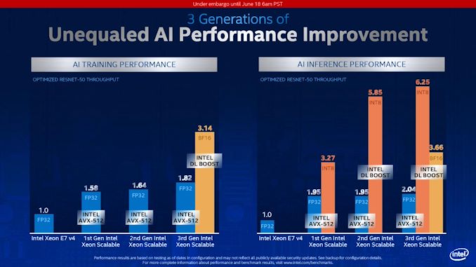
Normally we don’t post too many graphs of first party performance numbers, however I did want to add this one.
Here we see Intel’s BF16 DL Boost at work for Resnet-50 in both training and inference. Resnet-50 is an old training set at this point, but is still used as a reference point for performance given its limited scope in layers and convolutions. Here Intel is showing a 72% increase in performance with Cooper Lake in BF16 mode vs Cooper Lake in FP32 mode when training the dataset.
Inference is a bit different, because inference can take advantage of lower bit, high bandwidth data casting, such as INT8, INT4, and such. Here we see BF16 still giving 1.8x performance over normal FP32 AVX512, but INT8 has that throughput advantage. This is a balance of speed and accuracy.
It should be noted that this graph also includes software optimizations over time, not only raw performance of the same code across multiple platforms.
I would like to point out the standard FP32 performance generation on generation. For AI Training, Intel is showing a 1.82/1.64 = 11% gain, while for inference we see a 2.04/1.95 = 4.6 % gain in performance generation-on-generation. Given that Cooper uses the same cores underneath as Cascade, this is mostly due to core frequency increases as well as bandwidth increases.
Deployments
A number of companies reached out to us in advance of the launch to tell us about their systems.
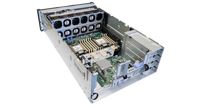
Lenovo will be announcing the launch of its ThinkSystem SR860 V2 and SR850 V2 servers with Cooper Lake and Optane DCPMM. The SR860 V2 will support up to four double-wide 300W GPUs in a dual socket configuration.
The fact that Lenovo is offering 2P variants of Cooper Lake is quite puzzling, especially as Intel said these were aimed at 4P systems and up. Hopefully we can get one in for testing.
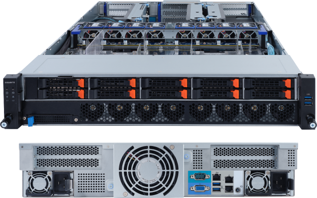
Also, GIGABYTE is announcing its R292-4S0 and R292-4S1 servers, both quad socket.
One of Intel’s partners stated to us that they were not expecting Cooper Lake to launch so soon – even within the next quarter. As a result, they were caught off guard and had to scramble to get materials for this announcement. It would appear that Intel had a need to pull in this announcement to now, perhaps because one of the major CSPs is ready to announce.

