Original Link: https://www.anandtech.com/show/1104
NVIDIA's Back with NV35 - GeForceFX 5900 Ultra
by Anand Lal Shimpi on May 12, 2003 8:53 AM EST- Posted in
- GPUs
NVIDIA made two poor bets a couple of years back that led to the lackluster introduction of the GeForceFX 5800 (NV30).
The first mistake was one that has been widely covered - the decision to go with a 0.13-micron manufacturing process. NVIDIA assumed that TSMC's 0.13-micron process would be much more mature than it was when NV30 was ready to go to production; in the end, a 0.13-micron process that lacked maturity held the NV30 back many more months than it needed to be.
The second mistake NVIDIA made with NV30 was in their assumption that flip chip packaging technology would not be ready by the scheduled introduction of the NV30. Without a flip chip package, NVIDIA did not think that a 256-bit memory interface would be a viable option and thus chose to outfit the NV30 with a 128-bit memory interface.
Both of these mistakes combined with drivers that were still in their infancy led to a very disappointing introduction of the GeForceFX. Not being the type of company to just fade away, NVIDIA immediately shifted their focus to NV35 even before NV30 hit the shelves. The end result was everything the NV30 should have been:
| - |
Manufacturing
Process
|
Architecture
|
Price
at Introduction
|
Core
Clock
|
Memory
Size
|
Memory
Bus
|
Memory
Clock
|
Memory
Bandwidth
|
| ATI Radeon 9800 Pro 256MB |
0.15-micron
|
DX9
|
$499
|
380MHz
|
256MB
|
256-bit
|
350MHz
|
22.4GB/s
|
| ATI Radeon 9800 Pro 128MB |
0.15-micron
|
DX9
|
$399
|
380MHz
|
128MB
|
256-bit
|
340MHz
|
21.8GB/s
|
| NVIDIA GeForceFX 5900 Ultra (NV35) 256MB |
0.13-micron
|
DX9
|
$499
|
450MHz
|
256MB
|
256-bit
|
425MHz
|
27.2GB/s
|
| NVIDIA NV35 128MB |
0.13-micron
|
DX9
|
$399
|
???MHz
|
128MB
|
256-bit
|
???MHz
|
???GB/s
|
| NVIDIA NV35 Value 128MB |
0.13-micron
|
DX9
|
$299
|
???MHz
|
128MB
|
???-bit
|
???MHz
|
???GB/s
|
| NVIDIA GeForceFX 5800 Ultra (NV30) |
0.13-micron
|
DX9
|
$399
|
500MHz
|
128MB
|
128-bit
|
500MHz
|
16GB/s
|
Just by looking at the table above you can see that NVIDIA was able to use slower (and cheaper) memory with the NV35, as well as drop the core clock a bit in comparison to the NV30. Will the architectural enhancements and 256-bit memory bus be able to overcome these reductions? You better believe it and soon you'll find out exactly how. Also note that NVIDIA is planning on introducing cheaper 128MB versions of the NV35 core in the next month.
Today we're finally able to bring you all there is to know about NVIDIA's latest GPU and the new GeForceFX 5900 Ultra.
As if that weren't enough, today we've got a special treat for you all as well. You may have heard of a game called "Doom3" and later on in this review you'll see a total of 8 GPUs compared using a current build of the game.
Let's get to it…
The Problem with Understanding Graphics
When NVIDIA introduced the GeForceFX, quite a ruckus ensued around the possibility that the NV30 did not have 8 distinct pixel rendering pipelines and in fact only had 4.
ATI quickly capitalized on the revelation and changed all of their marketing docs to point out the fact that their R3x0 GPUs had twice as many pipelines as NVIDIA's flagship. The community screamed foul play and NVIDIA was chastised, but the ironic part of it all was that the majority of the stones that were thrown were based on poor information.
In fact, the quality of information that has been coming from both ATI and NVIDIA in recent history has deteriorated significantly. Whereas companies like AMD and Intel are very forthcoming in the details of their microprocessor architectures, ATI and NVIDIA are very cryptic when they discuss their GPUs. The matter is further complicated by the introduction of marketing terms like "vertex engines" and referring to some parts of the GPU as a "pipeline" and others not when they both actually are "pipelines."
Now that GPUs are becoming much more like CPUs it is important that we understand the details of their architecture much like we do CPUs. You will find discussions in our forums revolving around the Pentium 4's 20 stage pipeline, but the closest parallel in the graphics discussions are about counting pixels.
We can understand why both ATI and NVIDIA are much less forthcoming with information than their counterparts in the CPU industry; remember that a new microarchitecture is introduced every five years in the CPU world, whereas the same occurs in the GPU world every 6 - 12 months. ATI and NVIDIA have to be very protective of their intellectual property as revealing too much could result in one of their innovations being found in a competitor's product 6 months down the road.
With that said, with this article we decided to dive in a little deeper into the GPU and begin drawing some parallels to what we know from our experience with CPUs. If you're not interested in learning how these GPUs work feel free to skip right ahead, otherwise grab some popcorn.
The Graphics "Pipeline"
The term "pipeline" is thrown around more in the graphics world than in any other business, yet there is quite a bit of misunderstanding (and misuse) involving the word. Graphics manufacturers used to refer to how robust their architecture is by counting the number of "rendering pipelines." The advent of the GPU brought about the use of the word "engine" in referring to anything that did any processing in the GPU - for example, the vertex engines would feed the pixel rendering pipelines. But to properly understand exactly what's going on in a GPU we have to take a step back and begin characterizing GPUs and their architecture not in marketing terms, but in actual microarchitectural terms. With that in mind, let's have a quick look at what a pipeline actually is.
Regardless of whether we're talking about a GPU or a CPU, the word pipeline still means the same thing. The analogy that's often used is one of an assembly line in a car manufacturing plant; instead of having everyone in the plant work on putting a single car together at the same time, the process is split into multiple stages. The frame is welded together at the welding station and then sent down the assembly line to the next stage where the doors may be put on then onto another stage where the engine would be dropped in and so on and so forth. The benefit of the assembly line is that you don't have to wait for one car to be finished in order for the next to begin assembly, as soon as the first car leaves that first stage, the next car begins the building process. This concept of an assembly line is identical to the concept of a pipeline; instead of waiting until one operation is complete before beginning on the next one, a pipelined processor splits its work up into multiple stages in order to have multiple instructions "in flight" at the same time.
The most basic pipeline in the CPU world is the classic five-stage integer pipeline, which consists of the following stages:
Instruction Fetch - Grab instructions from the program to be executed
Instruction Decode - Figure out what the instruction wants the processor to
do
Fetch Data/Operands - Grab any data needed for the instruction out of memory
(e.g. A = B + C, find the values of B and C so we can add them)
Execution - Carry out the actual operation (add B and C together)
Write Back - Write the result back to a register or memory (store the final
value of A somewhere)
Obviously today's microprocessors are significantly more complicated than the basic five stage pipe we just described, but the foundation for all pipelined microprocessors is the same - including GPUs.
The graphics pipeline isn't much different than the simple five-stage integer pipe we just described, however it contains an obscene number of stages. If you thought the Pentium 4's 20-stage integer pipeline was long, hearing that a graphics pipeline can consist of multiple hundreds or even thousands of stages may seem a bit strange. Luckily for GPUs, they have enough memory bandwidth and a pipeline-friendly set of data that prevents this excruciatingly long pipeline from being a performance-limiting characteristic.
The Graphics "Pipeline" (continued)
The incredibly long graphics pipeline can be summarized into six general stages, which we'll further dive into later in this article.
1) Instruction Fetch/Decode, DMA, etc…
This stage is one that receives instructions and commands from the driver and decodes them into operations for all other parts of the graphics pipeline to perform. This is the stage that tells all of the other countless stages what to do.
2) Vertex Processing
Now that the GPU knows what data it needs to begin processing and what it needs to actually do to this set of data, it starts working. The data sent to the GPU is sent in the form of the vertices of the polygons that will eventually be displayed on your screen. The first actual execution stage in the graphics pipeline is what has been referred to as T&L for the longest time. This is the transformation of the vertex data that was just sent to the GPU into a 3D scene. The transformation stage requires a lot of highly repetitive floating-point matrix math. Next comes the actual lighting calculations for each of these vertices. In a programmable GPU these initial vertex processing stages are very flexible in that short vertex shader programs can be written to control a number of the characteristics of the vertices to change the shape, look or behavior of a model among other things (e.g. matrix palette skinning, realistic fur, etc..). This stage is actually a pipeline of its own, split into a number of smaller stages.
3) Triangle Setup
After we have beautifully transformed and lit vertices it's time to actually generate some pixels so they can be displayed on your screen. But before that there's a bit of house keeping to be done. There are the culling and clipping stages that basically remove all the vertices that extend beyond the bounds of the scene. Then we have some of the nifty visibility calculations that go on in most of today's GPUs to help throw out vertices that won't be visible to the user. This is where technologies such as HyperZ and NVIDIA's Visibility Subsystem come into play to throw out data before we actually start rendering pixels and waste fill-rate and memory bandwidth. Here the vertices are transformed into primitives (e.g. triangles).
4) Rasterization
Now that we've had our spring cleaning it's time to generate some pixels. The triangles we just generated are now converted into pixels in the viewport space which is the 2D space of your monitor; remember that although this is 3D rendering, you're still looking at a flat (2D) monitor. The z-buffer data (how far away/deep the pixels are in reference to the viewer) is calculated and stored as well in order to turn this otherwise 2D image into a 3D world.
5) Shading & Texturing
Although shading and texturing are two separate stages, they are tightly coupled and occur in parallel. These stages are also pipelines of their own, but as we just mentioned they occur in parallel. Texture coordinates are calculated which will be used to map textures onto these polygons that have been created using the vertex data. The textures are then loaded and then we have the pixel shading stage where today's programmable GPUs can allow small programs to run and create neat looking effects on the pixels (e.g. shadow mapping, z-correct bump mapping, etc…). There is a bypass/feedback network that exists between these pipelines so that data from one pipe may be fed back into a different pipe in order to perform additional rendering passes, shading calculations, etc…
6) Raster Operations
This stage is where all pixel level operations occur, such as z/color/stencil rendering, as well as anti-aliasing and texture filtering.
7) DRAM accesses/Put it on the Screen
At the end of the pipeline we have all final DRAM accesses that must take place so we can write these pixels we've worked so hard at generating to memory before sending the data off to the RAMDACs or TMDS transmitter(s) for display on your monitor.
Now that you've got a general idea of the overall 3D pipeline, let's further
dive into each stage and see how the NV35 (GeForceFX 5900 Ultra) and the R350
(Radeon 9800 Pro) are similar and different, architecturally.
Stage 1: "The Front End"
The first stage of the graphics pipeline, as we mentioned before, is the initial stage where the application (in most cases a game) communicates with the API/driver and in turn talks to the GPU.
Instructions from the game being run are sent to the API, telling it to tell the hardware what the game wants to do. The API then interfaces with the graphics driver and passes on the API code. There is a real-time compiler in the graphics driver that takes the API code and essentially maps it to instructions that the particular GPU can understand, this is the first place where ATI and NVIDIA are divided. While both ATI and NVIDIA have the same approach, ATI's real-time compiler obviously generates instructions that only their GPUs can understand, while NVIDIA's compiler is tailored to NVIDIA GPUs only; makes sense, no?
What is contained in these instructions that are sent to the GPU? For all pre-DX8 code ("non-programmable"), vertices, indeces, commands that instruct the GPU where to go fetch vertices/indeces from or states (e.g. z-buffer enable/disable, texture filtering mode = trilinear, etc…) are the types of instructions you can expect to see in this stage. As we mentioned in our overview of the graphics pipeline, this stage mainly tells all of the other stages what to do, which is exactly what's happening here.
For DX8/DX9 code things are a bit different, as there are actual vertex/pixel programs that are sent to the driver and then mapped to GPU machine code. The difference between this approach and pre-DX8 code is that pre-DX8 code would trigger a series of events that would happen in the pipeline (e.g. lookup this texture, apply it to these pixels, repeat, etc…) whereas DX8/DX9 code offers much more flexibility for the programmer. Now the developer can tell the vertex shader FPUs to perform any task they would like, even to the point of coding non-graphics programs to run on the GPU. When DX8/DX9 code is sent to the GPU, the processor acts much more like a conventional CPU; a GPU running DX8/DX9 code is a lot like a CPU running any application you would on your computer.
Both ATI and NVIDIA are very stringent on details involving these front end stages of their pipelines, but as you can guess it is quite difficult to compare the two here. The efficiency and performance of the driver's real-time compiler is extremely important to how well these first set of operations perform.
The one thing you have to keep fresh in your mind about the graphics pipeline is that many parts of the pipeline are extremely parallel in nature, and thus optimizing the amount of parallelism in the code the compiler generates is key to extracting the full performance potential out of any GPU. The compiler dictates what registers data will be stored in, it handles any and all bundling of instructions and as we just mentioned, attempts to extract as much Instruction Level Parallelism (ILP) from the code as possible.
If you've ever wondered how newer drivers can increase performance, improvements in the driver's real-time compiler are often the reason for performance gains. The beauty of having a real-time compiler in the driver is that we don't have to wait for applications to take advantage of the hardware (for the most part) for us to get a performance boost from a brand new architecture. This is in sharp contrast to how things work in the CPU world where it takes a number of revisions before an application is recompiled with optimizations for a brand new CPU architecture. The graphics world will continue to use real-time compilers until the shader programs grow to be long enough that compiling at runtime is impossible, but it seems like that's going to be some time from now.
Along these lines, a good deal of the performance improvement with the new Detonator FX drivers is due to compiler optimizations for the new NV3x architecture. The next question is who makes a better compiler - ATI or NVIDIA? Compiler research and development is definitely new stomping grounds for both companies, but one thing is for sure, the more experience any driver team has with a new architecture, the better their compiler will be. In the case of ATI, they have been working on the R3xx compiler on real hardware since July of last year, whereas NVIDIA hasn't had nearly as much time with NV3x. The other factor aside from raw experience, is which driver team is more talented. We'll leave that one alone as we're not here to review resumes...
Stage 2: Vertex Processing
At the forefront of the 3D pipeline we have what has commonly been referred to as one or more vertex engines. These "engines" are essentially a collection of pipelined execution units, such as adders and multipliers. The execution units are fairly parallelized, to the point where there are multiple adders, multipliers, etc… in order to exploit the fact that most of the data they will be working on is highly parallel in nature.
The functional units that make up these vertex engines are all 32-bit floating point units, regardless of whether we're talking about an ATI or NVIDIA architecture. In terms of the efficiency of these units, ATI claims that there is rarely a case when they process fewer than 4 vertex operations every clock cycle, while NVIDIA says that the NV35 can execute at least 3 vertex operations every clock cycle but gave the range from 3 - 4 ops per clock.
It's difficult to figure out why the discrepancy exists without looking at both architectures at a very low level, which as we mentioned at the beginning of this article is fairly impossible due to both manufacturers wanting to keep their secrets closely guarded.
An interesting difference that exists between the graphics pipeline and the CPU pipeline is the prevalence of branches in graphics code. As you will remember from our articles detailing the CPU world, branches occur quite commonly in code (e.g. 20% of all integer instructions are branches in x86 code). A branch is any piece of code where a decision must be made and the outcome of which determines which instruction to execute next. For example, a general branch would be:
If "Situation A" then begin executing the following code
…
Else, if "Situation B" then execute this code
…
As you can guess, branches are far less common in the graphics world. Extremely complex lighting algorithms are much more likely to contain branches than any other sort of code as well as vertex processing in general. Obviously in any case where branches exist, you will want to be able to predict the outcome of a branch before evaluating it in order to avoid costly pipeline stalls. Luckily, because of the high bandwidth memory subsystem that GPUs are paired up with as well as the limited nature of branches in graphics code to begin with, the branch predictors in these GPUs don't have to be too accurate. Whereas in the CPU world you need to be able to predict branches with ~95% accuracy, the requirements are no where near as stringent in the GPU world. NVIDIA insists that their branch predictor is significantly more accurate/efficient than ATI's, however it is difficult to back up those claims with hard numbers.
Stages 3 & 4: Triangle Setup & Rasterization
We've explained basically what happens in these two stages, but with the NV35 NVIDIA introduced another method to save processing power that would otherwise occur in the next stage of the pipeline.
With the next-generation of games, shadows will become increasingly more complicated due to complex lighting algorithms. Along the lines of technologies such as HyperZ or general occlusion culling, NVIDIA has outfitted the NV35 with something they like to call "UltraShadow."
The UltraShadow technology is fairly simple in practice; a developer just needs to specify boundaries for an object, indicating the region that a shadow would be cast upon based on a particular light source. These boundaries then become the limits for any shadow calculations, and thus excess processing is avoided as you can see from the image below.
Stage 5: Shading/Texturing
The shading/texturing stage is single handedly responsible for the most amount of confusion in the GPU world these days. Originally, before the advent of the programmable GPU (DX8/DX9 class hardware), this stage consisted of reading pixels, texturing them (through the use of register combiners) and either looping the process or passing them on to the next stage. In those days, it was very easy to define how many pixels you could send through this stage in a given clock and what the throughput of this stage would be.
As we've made it a point to mention, each individual stage of the graphics pipeline is actually composed of multiple individual pipeline stages, this shading/texturing stage is no different. Before the days of programmable GPUs, the number of pixels in/out of this stage was fairly fixed and thus the marketing folks started recognizing these pipelines as rendering pipelines in the graphics core. The more pixels you could pass through this stage in parallel, the more robust your hardware. It provided an excellent way of differentiating previous generation hardware from the current generation; we saw consumer graphics evolve from a single pixel pipe to two, to four and eventually to eight.
The other method for classification ended up being the number of textures these pipelines could apply to a pixel passing through them in a given clock. We saw designs that were able to apply one, two or three textures per pixel, per pipe, per clock and thus the marketing folks were once again able to come up with nice terms such as pixel and texel fill rate (a way of representing the number of textured pixels a GPU could produce). However, once programmable GPUs began surfacing, it became much more difficult to characterize hardware by the number of pixel pipelines that exist in the GPU. In order to understand why, we must understand exactly what a "pixel pipeline" is.
Like most parts of the GPU, these pixel pipelines are nothing more than collections of execution units - adders, multipliers, etc… that have a specific task. There are significantly more execution units in a GPU than there are in a CPU; for example, the Pentium 4 features 3 general purpose floating point units (FPUs), whereas the NV35 features a total of 32 FPUs in its shading/texturing stage alone. The difference between the two is that the NV35's FPUs are much more specialized than what you'd encounter in a general purpose CPU like the Pentium 4 or Athlon XP.
Since programmable GPUs are going to have to execute custom code in the form of shader programs as well as perform the usual texture-and-go functionality of the old days, it has become much more difficult for marketing folks to characterize exactly how many "pixel pipes" exist in modern GPUs.
The number of pixel pipes has always been related to the number of pixels you could spit out every clock cycle; now, with the introduction of fully programmable pipelines that number can vary rather significantly depending on what sort of operations are carried out through the pipe.
Think of these pixel rendering pipelines, not as independent pathways, but as a farm of execution resources that can be used in any way. There are a number of adders that can be used either in parallel, or in series, with the result of one being fed to the input of another. If we were to characterize the number of pipelines by the number of pixels we could send through there in parallel then we could end up with numbers as low as 2 or as high as 16.
What the marketing folks have done to help clear up the confusion is come up with a list of scenarios and the throughput of their GPUs in those scenarios; for example, the following chart from NVIDIA:
As you can see, there is sufficient hardware in the NV35 to guarantee a throughput of 8 pixels per clock in most scenarios, but in older games (e.g. single textured games) the GPU is only capable of delivering 4 pixels per clock. If you correctly pack the instructions that are dispatched to the execution units in this stage you can yield significantly more than 8 pixel shader operations per clock. For example, in NVIDIA's architecture a multiply/add can be done extremely fast and efficiently in these units, which would be one scenario in which you'd yield more than 8 pixel shader ops per clock.
It all depends on what sort of parallelism can be extracted from the instructions and data coming into this stage of the pipeline. Although not as extreme of a case (there isn't as much parallelism in desktop applications), CPUs enjoy the same difficulty of characterization. For example, the AMD Athlon XP has a total of 9 execution units, but on average the processor yields around 1 instruction per clock; the overall yield of the processor can vary so much depending on available memory bandwidth and the type of data it's working on among other things.
ATI's R3xx architecture differs from NVIDIA slightly in this respect, as they are able to output 8 pixels per clock in every one of the situations listed above. The advantage isn't huge as it is mostly limited to older games, but the difference does exist and is worth pointing out.
Let's talk precision (Stage 5 continued)
Historically the vertex engines have been composed of floating point units for much longer than the pixel pipes have been; remember, we're thinking about these stages not in generic marketing terms but in their true existence - as functional units.
With the transition to DX9 hardware came the move to floating point units in the shading/texturing stages. FPUs can provide greater precision (try representing 1.04542 as anything other than a decimal number and still retain full precision) but at the cost of much larger and more expensive hardware, primarily an increase in transistor count and die size. We've discussed the merits of FP precision in previous articles, for more information on what you can do with FP support hop over here.
Once again here's where the marketing folks do the industry a severe injustice when it comes to talking about the "precision" of these FPUs. Precision, when referring to any sort of floating point number, is given in the number of bits allocated to representing that number. In the case of DirectX 9, there are two modes that are supported - full and half precision.
Full precision, according to Microsoft's spec, calls for 24-bit representation for each color component for a total of 96-bits to represent each pixel. The DX9 specification also calls for partial precision support with 16-bit components, for 64-bit representation of every pixel. ATI's R3xx hardware supports both of these modes and helped define them in the original specification.
NVIDIA does things a little differently; they support the 16-bit partial precision mode, however their NV3x hardware does not support the 24-bit full precision mode. Instead, NVIDIA supports the IEEE-754 spec which calls for 32-bits of precision; this is not included as part of the DirectX 9 specification.
So when ATI mentions that NVIDIA does not support "full precision" they are, in some respects, correct - NVIDIA does not support the 24-bit precision mode as defined by Microsoft, they support a mode with greater precision. The question is, if a game doesn't request partial precision, what does NVIDIA's hardware do? According to NVIDIA, the NV3x will default to 32-bit precision unless requested to render in partial precision (16-bit) mode.
Now that we've got the precision issue squared away, let's talk about speed. Does executing in full precision occur any faster than if you execute in partial precision? The design of both ATI's and NVIDIA's hardware dictates that there is only one set of FPUs for the shading/texturing stage, and all operations regardless of their precision go through this set of FPUs. On ATI's R3xx GPUs this means that there are clusters of 4 x 24-bit FPUs, while on NVIDIA's NV3x GPUs there are clusters of 4 x 32-bit FPUs. All operations on these FPUs occur at the same latency, regardless of precision. So whether you're doing a 16-bit add or a 24/32-bit add, it occurs at the same rate.
The only penalty to using higher precision is of course in regards to memory bandwidth and memory size. So while it has been claimed in the past that full precision can only be had at the expense of speed, this isn't true from a computational standpoint, only from the perspective of the memory subsystem.
Stages 6 & 7: Raster Operations & DRAM accesses
The final stages in the 3D pipeline have been explained by us in the past on numerous occasions, so we will just touch on the enhancements as they apply to NV35.
First and foremost, NVIDIA's compression algorithms have been improved tremendously with the NV35 so that the biggest performance gains you will see will be in high resolution Anti-Aliasing modes; NVIDIA appropriately calls this their Intellisample High-resolution Compression Technology (HCT).
The next major improvement is the introduction of a 256-bit wide memory bus to the NV35. NVIDIA originally thought that BGA memory and flip-chip packaging technology would not be ready for prime time by NV30's introduction date and thus outfitted the original chip with no more than a 128-bit wide memory interface. The biggest challenges that exist with a 256-bit wide memory interface are routing related; routing traces to/from the GPU and to/from the individual memory chips themselves. Both flip chip packaging on the GPU side and BGA packaging on the memory side made a 256-bit memory interface an attainable reality, even on NV30.
Obviously with NV30 heavily delayed, NVIDIA didn't want to push things back even further to wait on a re-spin of the design with a wider memory bus, but with NV35 we finally have that 256-bit memory interface we've been craving.
Fixing Anisotropic Filtering
Not too long ago I flew down to NVIDIA in Santa Clara to meet with them for the purpose of discussing image quality. As you will remember from our NV30 review, we were far from pleased with the way NVIDIA's anisotropic filtering looked in comparison to ATI's.
Luckily with the latest drivers from NVIDIA that accompany the NV35, the problem has been solved. Let's first start off with all of ATI's modes:
| ATI Radeon 9800 Pro - Anisotropic Filtering Comparison | |
 2X Performance |
 2X Quality |
 4X Performance |
 4X Quality |
|
|
 8X Quality |
 16X Performance |
 16X Quality |
Fixing Anisotropic Filtering (continued)
Next we have NVIDIA's modes
| NVIDIA GeForceFX 5900 Ultra- Anisotropic Filtering Comparison | |
 2X High Performance |
 2X Performance |
 2X Quality |
|
 4X High Performance |
 4X Performance |
 4X Quality |
|
 8X High Performance |
 8X Performance |
 8X Quality |
|
Comparing Anisotropic Filtering
Now we can compare ATI's modes to NVIDIA's modes, head to head:
| ATI's Performance Aniso Mode vs. NVIDIA's High Performance Aniso Mode | |
 ATI 8X Performance |
NVIDIA 8X High Performance |
Here we see that ATI's Performance mode appears to be a bit better than NVIDIA's High Performance mode. Let's have a look at the mip bands to see a better idea of what's going on:
ATI 8X Performance
NVIDIA 8X High Performance
The transitions between mip bands is smoother on the NVIDIA setting.
Comparing Anisotropic Filtering (continued)
| ATI's Performance Aniso Mode vs. NVIDIA's Performance Aniso Mode | |
|
ATI 8X Performance |
NVIDIA 8X Performance |
It's a close call between these two, let's color those mip bands:
ATI 8X Performance
NVIDIA 8X Performance
Finally, NVIDIA's claim that their "performance" mode offers equal to or greater quality than ATI's is actually true. The benefit here is that NVIDIA actually does some (albeit a small amount) of trilinear filtering in their performance aniso mode, which smooths the transitions between the different mip levels. The tables have turned and now it's ATI's turn to play catch-up and make their performance mode look better.
Comparing Anisotropic Filtering (continued)
| ATI's Quality Aniso Mode vs. NVIDIA's Quality Aniso Mode | |
|
ATI 8X Quality |
NVIDIA 8X Quality |

ATI 8X Quality
NVIDIA 8X Quality
Both ATI and NVIDIA's quality modes are virtually identical, you'd be hard pressed to find a difference between the two.
New Drivers from ATI & NVIDIA
Both ATI and NVIDIA provided us with new drivers for this review; ATI gave us their new Catalyst 3.4 drivers while NVIDIA provided us with their new Detonator FX drivers (44.03).
The Catalyst 3.4 drivers provided us with a couple of problems, the most noticeable ones were the following:
1) Performance under Doom3 was horrible, significantly lower than the older Catalyst 3.2 drivers. These drivers would also cause the game to crash in a repeatable fashion.
2) Update: The Splinter Cell issues we reported in the past are in fact an issue with Splinter Cell and enabling AA. The issues seemed to happen more with ATI because NVIDIA's drivers disable AA in Splinter Cell, hence they seemed to be related to ATI's drivers.
NVIDIA's Detonator FX drivers will be publicly available on May 14th and will improve performance across the board for all FX cards, we will be following up with a performance article later this week entailing the exact performance improvements you can expect from the Detonator FX drivers. We encountered no issues with the drivers, and we're glad NVIDIA finally changed their anisotropic filtering quality settings to match up with ATI's (as well as fix the image quality issues we've been griping about all this time):
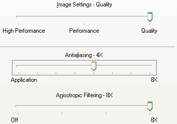
Finally, we can have an apples-to-apples comparison between ATI & NVIDIA
aniso modes
New Cards from ATI & NVIDIA
If you think the only new card we have in our hands is the GeForceFX 5900 Ultra, you've got another thing coming. ATI is also introducing a 256MB version of their Radeon 9800 Pro:
ATI had to double the number of memory chips on the board and moved to 350MHz DDR-II SDRAM, up from the original 340MHz DDR-I SDRAM used on the 128MB Radeon 9800 Pro. Despite the increase in memory clock, the move to more memory chips actually reduced performance a bit (the 256-bit bus now must be split among twice as many chips, which does create some overhead) and when combined with the increased memory clock the end result is that the Radeon 9800 Pro 256MB is no faster in most cases than the 128MB version.
Twice as much memory, twice as many chips, a higher memory clock - but identical
performance to the 128MB card is what the $499 Radeon 9800 Pro will get you
We encountered some memory artifacts at random periods during our testing of the Radeon 9800 Pro, especially during our Doom3 testing. We're assuming this is due to the engineering sample nature of our review hardware and that ATI will fix the issue before mass production.
New Cards from ATI & NVIDIA: The GeForceFX 5900 Ultra
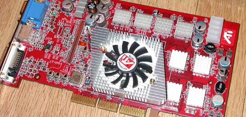
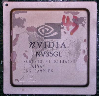
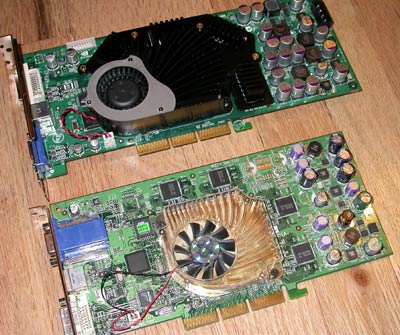
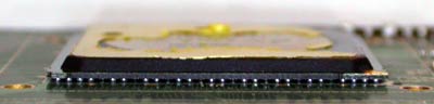
You've made it all this way and haven't gotten a good look at the first incarnation of NVIDIA's NV35 - the GeForceFX 5900 Ultra:
The first thing you'll notice is that the heatsink/fan has changed dramatically from the NV30. The extremely loud and annoying fan noise is thankfully gone, and the fan is actually virtually silent in 2D mode; the fan is considerably louder than a Radeon 9800 Pro's fan in 3D mode however. For those of you that are curious, the reason for the annoying sound created by the NV30's fan was because the fan actually was improperly designed and physically rubbed up against its shroud, causing the annoying sound we brought you in a movie clip in our NV30 review.
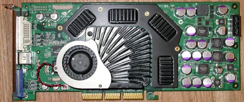
The only problem we encountered with our GeForceFX 5900 Ultra board was that the analog video output was incredibly blurry. For a $499 card we would expect better, and we can only hope that shipping cards won't have the horrible output we noted on our reference board. We do have high hopes that the problem will be fixed as the board that we had will change considerably before hitting mass production, for starters, the card is supposed to be as long as a GeForce4 Ti 4600 in its final revision:
The NV35 board may end up losing close to an inch off of its length by the time
it hits store shelves
As we mentioned before, NVIDIA will be launching two 128MB boards based on the NV35 core priced at $399 and $299 and varying based on clock speeds.
Sneak Peek at the New GeForceFX 5600 Ultra
Since NVIDIA gave us the ok to publish Doom3 numbers from the shipping revision of the GeForceFX 5600 Ultra, we are able to give you a quick look at what has changed since we first reported on the 5600 Ultra.
The shipping version of the GeForceFX 5600 Ultra will use a flip chip package on the GPU (much like the NV30/35) and thus NVIDIA was able to hit higher clock speeds with this card, thus making it more competitive with the Radeon 9600 Pro. We will be bringing you a full review of the final shipping card next week, but for now here are some teaser pics:
|
The
old NV31
|
The
new NV31
|
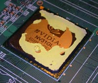 |
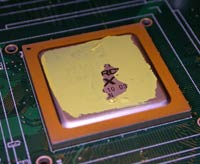 |
Old NV31

New NV31 - Note the heatspreader on top of the flip chip package for improved
cooling
The Test
|
Windows
XP Professional Test Bed
|
|
|
Hardware
Configuration
|
|
| CPU |
Intel
Pentium 4 3.00GHz (Hyper-Threading Enabled)
|
| Motherboard |
Intel
D875PBZ - Intel 875P Chipset
|
| RAM |
2
x 256MB DDR400 Corsair DIMMs
|
| Sound |
None
|
| Hard Drive |
120GB
Western Digital Special Edition 8MB Cache HDD
|
| Video Cards (Drivers) |
All ATI Cards used
Catalyst 3.4 drivers |
Unless otherwise noted, all tests were conducted with 4X Antialiasing and 8X Quality Anisotropic Filtering; you don't buy a $500 video card only to leave these settings disabled.
Sneak Preview - Doom3 Performance
What's the most frustrating part of talking about all this high-power DX9 hardware? There are absolutely no games available that truly stress it; the market is waiting for the release of one very pivotal title, the game that will determine whether ATI or NVIDIA is crowned the true next-generation performance king: Doom3.
We have been anxiously awaiting the release of a pre-release benchmark version of Doom3 for our graphics tests, and last Thursday we were given a unique opportunity to benchmark Doom3 on a number of the latest GPUs. The opportunity was put together by idSoftware and NVIDIA, and was very limited in nature, but it was something we had to jump on.
We were given one evening with a system running Doom3, to test the latest GPUs from both ATI and NVIDIA using whatever drivers we pleased using whatever settings we would like. The only stipulation was that we could not comment on how the game looked, just on the performance of the GPUs. Doom3 is still a while away from shipping and thus we can understand id not wanting us to talk about the look of the game, and we gladly agreed to their terms in order to bring you a quick look at the performance of Doom3 on today's GPUs.
Here are some words of forewarning though; for starters, neither ATI nor NVIDIA gave us Doom3 optimized drivers to test with, we tested using the same drivers we used in all of our other tests (both drivers will be publicly available next week from ATI and NVIDIA). We actually ended up using ATI's Catalyst 3.2 instead of 3.4 for our Doom3 tests simply because the Catalyst 3.4 drivers we had were significantly slower in Doom3 and were much more unstable than the 3.2 release.
NVIDIA obviously wouldn't agree to this opportunity unless they knew they would come out ahead in the benchmarks, and as you are soon to see, they did. John Carmack did have a few words of warning, which we received after our benchmarking time with the system was up:
"We have been planning to put together a proper pre-release of Doom for benchmarking purposes, but we have just been too busy with actual game completion. The executable and data that is being shown was effectively lifted at a random point in the development process, and shows some obvious issues with playback, but we believe it to be a fair and unbiased data point. We would prefer to show something that carefully highlights the best visual aspects of our work, but we recognize the importance of providing a benchmark for comparison purposes at this time, so we are allowing it to be used for this particular set of tests. We were not happy with the demo that Nvidia prepared, so we recorded a new one while they were here today. This is an important point -- while I'm sure Nvidia did extensive testing, and knew that their card was going to come out comfortably ahead with the demo they prepared, right now, they don't actually know if the demo that we recorded for them puts them in the best light. Rather nervy of them, actually.
The Nvidia card will be fastest with "r_renderer nv30", while the ATI will be a tiny bit faster in the "r_renderer R200" mode instead of the "r_renderer ARB2" mode that it defaults to (which gives some minor quality improvements). The "gfxinfo" command will dump relevant information about the functioning renderer modes and optimizations. At some point, after we have documented all of the options and provided multiple datasets, Doom is going to be an excellent benchmarking tool, but for now you can still make some rough assessments with it."
So although the game isn't finished and the drivers are not tuned, we should be able to get a decent idea of how performance is shaping up under Doom3. We were only able to test the following cards:
ATI Radeon 9800 Pro
ATI Radeon 9600 Pro
ATI Radeon 9200
NVIDIA GeForceFX 5900 Ultra
NVIDIA GeForceFX 5800 Ultra
NVIDIA GeForceFX 5600 Ultra
NVIDIA GeForceFX 5200 Ultra
The only options that we could change in game were the quality settings which we could set to low, medium or high. We benchmarked medium and high, but on the fastest cards the performance drop in high quality mode was negligible so we stuck to reporting the medium detail level scores due to time constraints.

id allowed us to publish a screenshot to give you an idea of the level of detail we're talking about with Doom3. The game is nothing short of impressive and makes the rest of our benchmark suite look extremely dated.
We ran at 1024x768, 1280x1024 and 1600x1200 with AA/Aniso off as well as with 4X AA and 8X Quality Aniso enabled.
Excited yet? Let's get to the results…
Doom3 Performance - No AA/Aniso
At 1024x768 the 5900 Ultra does extremely well, already breaking the 100 fps mark. What's interesting to note is how close the NV30 and NV35 are in this benchmark, indicating that raw GPU power not memory bandwidth is actually a limiting factor here.
Without any AA/Anisotropic filtering enabled, ATI's solutions fall siginficantly behind the NV30/35.
It's also worth noting that the new GeForceFX 5600 Ultra improves performance by 12% over the previous card we reviewed.
What's quite impressive is that even the mainstream cards are quite playable at 1024x768; with more driver tuning and turning down a few more image quality features (even at medium quality we're dealing with an extremely good looking setup) would make Doom3 even more playable on the cheaper cards.
As we crank up the resolution we see that the performance drop is significant, even the almighty NV35 falls a good 33%. The standings remain virtually unchanged, but it's clear that the mainstream cards will be limited to resolutions of 1024x768 and below, which isn't different from what we'd expect.
Given the slower paced nature of the game, even 1600x1200 may be considered playable for many gamers if you look at the performance of the 5900/5800 Ultra. Once again we see that the performance difference between the NV35 and NV30 isn't all that great, but let's see what happens when we crank up the AA/Aniso modes.
Doom3 Performance - 4X AA/8X Quality Aniso
With higher quality settings at our disposal, we went back to the benchmark (note: the Radeon 9200 was absent from these tests as we noted a number of rendering errors on the Radeon 9200):
Enabling the higher quality modes closes the gap between the Radeon 9800 Pro and the 5800 Ultra, but the 5900 Ultra continues to hold a healthy lead.
These high-res AA/Aniso modes are clearly not for the mainstream cards, and are even stressing the new $500 cards fairly well. Those looking for the best Doom3 performance may want to wait until right after the game comes out to upgrade their graphics cards, with hopes that even faster (and cheaper) hardware will be out by then.
Unreal Tournament 2003 Performance
Arguably the best looking game available today, Unreal Tournament 2003 continues to be a cornerstone of our GPU benchmarking suite. We continue to use the game's built-in benchmark.exe and force the maximum detail settings for every test run. Keep in mind we're only reporting flyby numbers, as the botmatch results are more CPU/platform bound than GPU bound.
The performance is very close between the 5900 Ultra and the Radeon 9800 Pro to the point where you wouldn't be able to notice a performance difference between the two. Here we have a perfect example of where having 256MB of memory isn't going to help you in today's games, but if you don't plan on upgrading your card for a couple of years then it absolutely makes sense to purchase one with as much memory as possible.
It is worth noting that the NV35 is a significant improvement from the NV30, on the order of 21% at 1024x768.
Quake III Arena
As we've mentioned in the past, the Quake III engine is still being used and thus performance using the engine shouldn't be ignored. For this reason we continue to use Quake III Arena as a benchmark, despite its insanely high performance results:
The GeForceFX 5900 Ultra does extremely well in Quake III Arena, to the point where it is CPU/platform bound at 1600x1200 with 4X AA/8X Anisotropic filtering enabled. Quake III is one situation where you could easily enable 6X or 8X AA settings without sacrificing playability, and it would be these rare situations where 256MB of memory would be necessary to deal with supporting such a large frame buffer.
Here we see a perfect example of the Intellisample HCT giving the NV35 core a serious performance advantage over the NV30.
Jedi Knight 2
With the recent announcement of a successor to Jedi Knight 2 in the works (also based off the Quake III engine), it makes sense for us to continue to use JK2 as a benchmark:
The performance standings under Jedi Knight II are similar to what we saw under Quake III Arena, but definitely not as extreme in favor of the NV35.
Comanche 4
Finally we leave off with Comanche 4, which gives the Radeon 9800 Pro its first significant lead over the 5900 Ultra in this review.
What's interesting is that we're finally able to see some sort of a performance advantage to having 256MB of memory in the 1600x1200 test, where the Radeon 9800 Pro 256MB is around 10% faster than the 128MB version - presumably because of the increase in memory size since we've already seen that the memory clock increase does nothing for the card's performance.
Final Words
What stood out the most about NVIDIA was how some of their best people could look us in the eye and say "we made a mistake" (in reference to NV30). When we first saw NV35 running last year we already had a much better taste in our mouths than what had been left after NV30; now after putting it through its paces, we can honestly say that NV35 is everything that was right about NV30 plus everything that was lacking in NVIDIA's first FX GPU.
The combination of a 256-bit memory bus, a more efficient architecture and more mature drivers has made this second round a lot stronger for NVIDIA. The balance of power has been shifted back towards NVIDIA, and with their driver problems solved the potential for NVIDIA to make a comeback across all market segments is quite high.
The Doom3 performance of the NV35 is definitely promising, especially considering that we benchmarked with an un-optimized driver. However a lot can change between now and the release of the game, it will be interesting to see how quickly ATI will incorporate Doom3 optimizations into their current drivers in the event that we get another such opportunity to benchmark Doom3 in the near future.
At a $499 price tag, the GeForceFX 5900 Ultra is extremely hard to justify, but the $299 and $399 parts may be interesting depending on the final clock speeds that NVIDIA decides upon. Quite possibly the most exciting part of today's launch is the release of NVIDIA's Detonator FX drivers that have finally solved the anisotropic filtering issues we were shocked to have with NVIDIA's hardware in the past. Later this week we will bring you a comparative review detailing the performance of all of the anisotropic filtering modes as well as a better idea of exactly how much performance the new Detonator FX drivers will bring you.
The new shipping GeForceFX 5600 Ultra with a flip chip package is also an intriguing possibility, as we expect it to be able to give the Radeon 9600 Pro much more competition than the original 5600 Ultra. This situation where the shipping product is much improved over the originally reviewed product is all too reminiscent of the Radeon 9500 Pro, whose performance changed dramatically after our initial performance preview. We will see in the coming weeks how the final 5600 Ultra stacks up across the board.
From the ATI camp the $499 Radeon 9800 Pro 256MB, just like the NV35, is a difficult purchase to justify; even more difficult in this case because the GeForceFX 5900 Ultra does outperform it in a number of tests. The benefit of 256MB of memory is quite small right now, and the price premium is definitely not worth it. We'd also honestly hope that the issues we encountered with our Radeon 9800 Pro 256MB board were limited to our board alone, and aren't representative of ATI running their memory out of spec.
There are rumors of an answer to NVIDIA's NV35 in the works for an introduction in the relatively near future based on the R3xx architecture. We'd assume this NV35 competitor to remain a 0.15-micron part, but with higher core clock speeds and maybe a few micro-architectural tweaks/enhancements to gain the performance edge on NVIDIA.
The next-generation of games are finally on their way, and it looks like we'll have an extremely powerful set of cards to choose from when titles like Doom3, Half-Life 2 and Deus Ex2 hit later this year.


